Semiconductor light emitting device

A technology of light-emitting devices and semiconductors, applied in semiconductor devices, electric solid-state devices, electrical components, etc., to achieve the effect of suppressing erroneous actions

Active Publication Date: 2014-04-16
SANKEN ELECTRIC CO LTD
View PDF6 Cites 3 Cited by
  • Summary
  • Abstract
  • Description
  • Claims
  • Application Information

AI Technical Summary

Problems solved by technology

[0004] However, in a field-effect transistor (FET) mounted on a silicon substrate as a driving device for a semiconductor light-emitting element, a PNP parasitic transistor may occur, and a current that cannot be controlled by a gate voltage may flow.
In addition, when a current flows through the substrate, an NPN parasitic transistor may be formed, and the FET may not operate normally.
Therefore, when the semiconductor light emitting element and the driving device are integrated on the same semiconductor substrate, the semiconductor light emitting device may not operate normally due to a malfunction of the driving device.

Method used


Image

  • Semiconductor light emitting device
  • Semiconductor light emitting device
  • Semiconductor light emitting device

Examples


Embodiment Construction

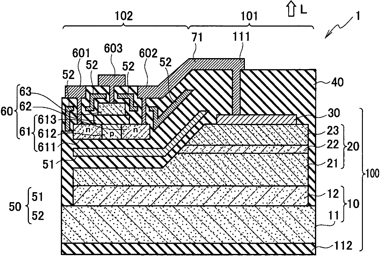
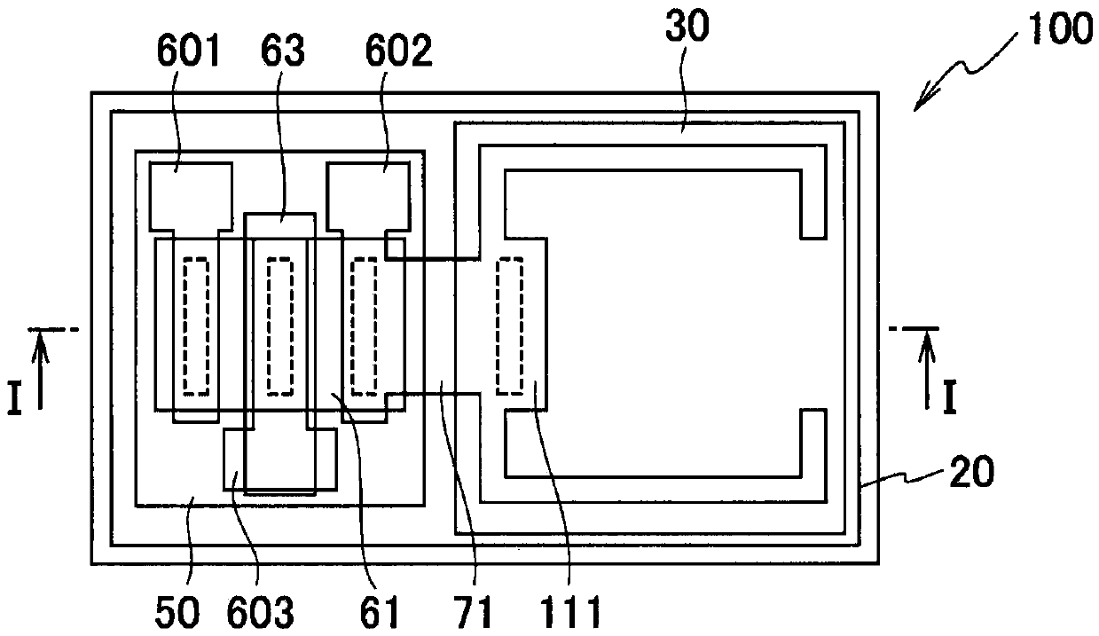
[0022] Embodiments of the present invention will be described with reference to the drawings. In the description of the drawings below, the same or similar symbols are given to the same or similar parts. However, it should be noted that the drawings are schematic, and the relationship between the thickness and planar dimensions, the thickness ratio of each layer, and the like are different from those in reality. Therefore, the specific thickness and size should be judged with reference to the following description. In addition, it is needless to say that the drawings also include parts in which the relationship and ratio of dimensions are different from each other.

[0023] In addition, the embodiments shown below are examples of devices and methods for embodying the technical idea of ​​the present invention. In the embodiments of the present invention, the materials, shapes, structures, arrangements, etc. of the structural components are not limited to the following . Vari...


PUM


Abstract

The present invention provides a semiconductor light emitting device which enables the semiconductor light emitting elements and a driving device to be configured on the same semiconductor substrate, and restrains the misoperation in the driving device. The semiconductor light emitting device comprises the semiconductor substrate defining a light-emitting area and a driving device area on a main surface; a laminating body configured to the driving device area from the light-emitting area continuously on the main surface of the semiconductor substrate, and possessing a structure formed by laminating an n-type semiconductor layer composed of an epitaxially growing nitrides semiconductor, an active layer and a p-type semiconductor layer orderly; an interlayer insulating film configured on the laminating body; a control transistor configured above the driving device area via at least one part of the laminating body and the interlayer insulating film and controlling the luminescence of the laminating body; and a shading film configured between the control transistor and the laminating body in the interlayer insulating film.

Description

technical field [0001] The present invention relates to a semiconductor light emitting device in which a semiconductor light emitting element and a driving device for the semiconductor light emitting element are arranged on the same semiconductor substrate. Background technique [0002] In a semiconductor light emitting device having a semiconductor light emitting element such as a light emitting diode (LED) or a semiconductor laser, the semiconductor light emitting device can be miniaturized by integrating the semiconductor light emitting element and a driving device for driving the light emitting element on the same semiconductor substrate. For example, a method has been proposed in which a semiconductor light emitting element is formed on a silicon substrate via a via layer, and a driving device for the semiconductor light emitting element is formed monolithically on the silicon substrate (for example, refer to Patent Document 1). [0003] [Patent Document 1] Japanese Pat...

Claims


Application Information

Patent Timeline
IPC IPC(8): H01L27/15
CPCH01L25/0753H01L33/42H01L33/48H01L33/62H01L2924/12041
Inventor 杉森畅尚
Owner SANKEN ELECTRIC CO LTD
Why Eureka
Try Eureka