Pin mapping method and system

A mapping method and mapping relationship technology, applied in special data processing applications, instruments, electrical digital data processing and other directions, can solve the problems of inaccurate pin mapping relationship, low efficiency, large workload, etc., and achieve accurate mapping relationship and efficiency. high effect

Active Publication Date: 2014-04-23
无锡亚科鸿禹电子有限公司
View PDF5 Cites 4 Cited by
  • Summary
  • Abstract
  • Description
  • Claims
  • Application Information

AI Technical Summary

Problems solved by technology

[0007] Embodiments of the present invention provide a pin mapping method and system to solve the problem that the mapping met

Method used


Image

  • Pin mapping method and system
  • Pin mapping method and system
  • Pin mapping method and system

Examples


Embodiment 1

[0060] First, introduce the motherboard and daughter board.

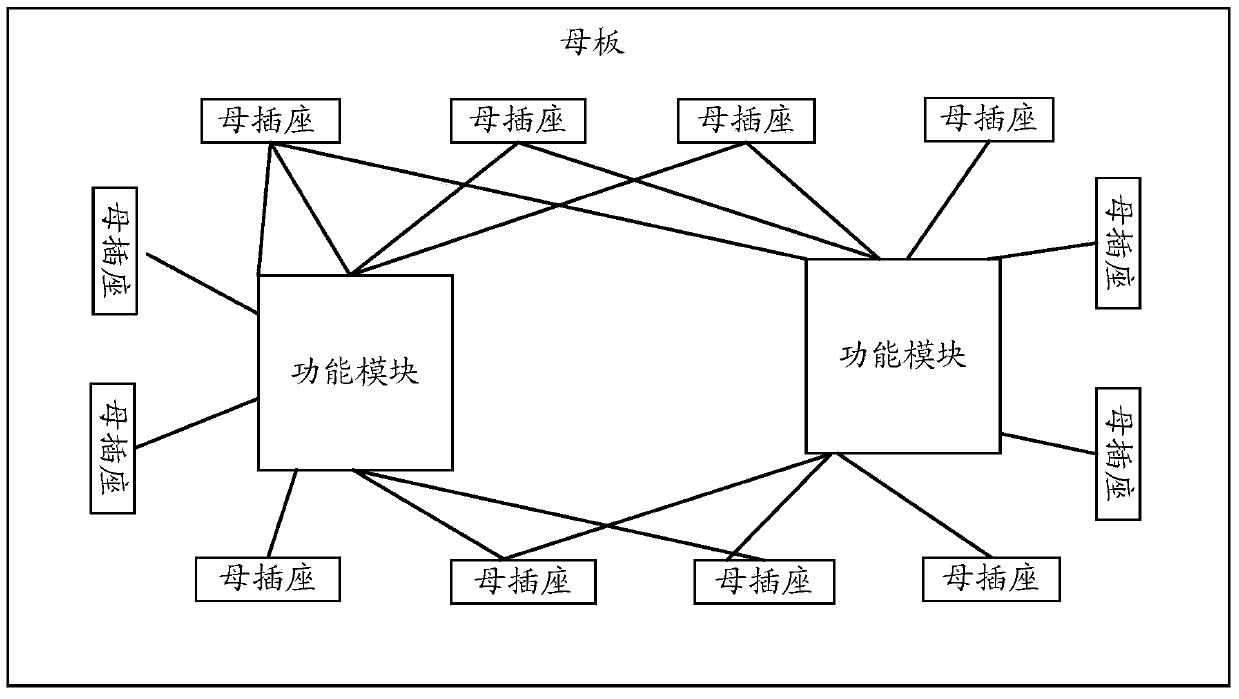
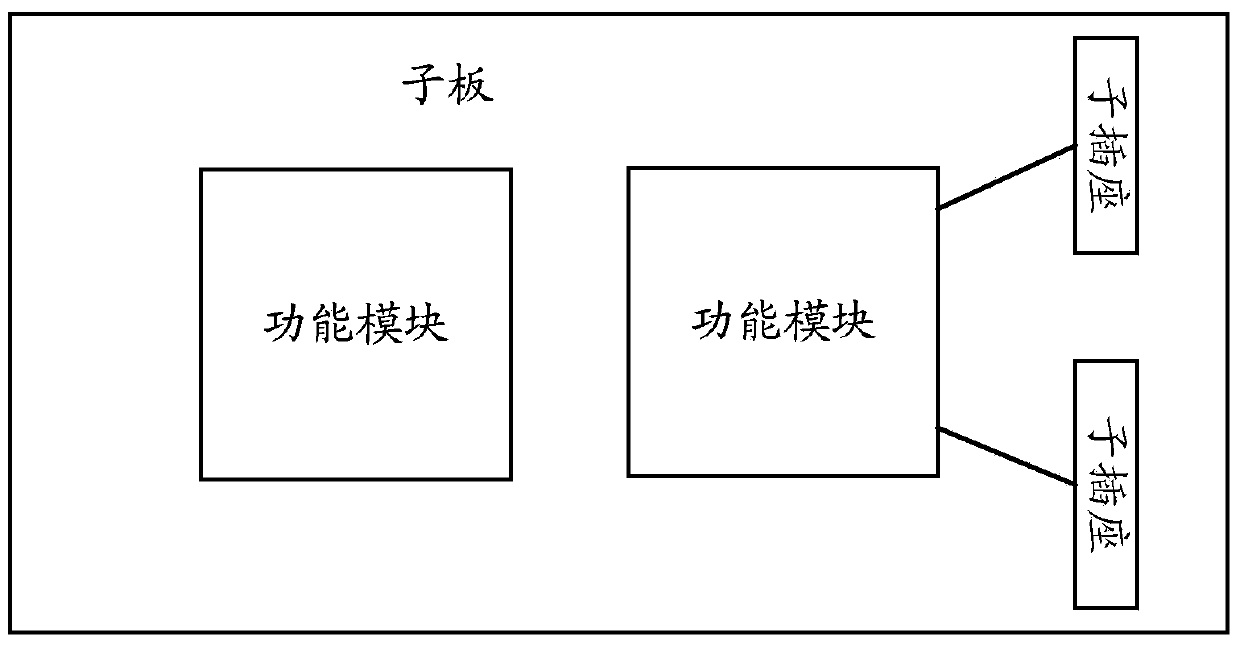
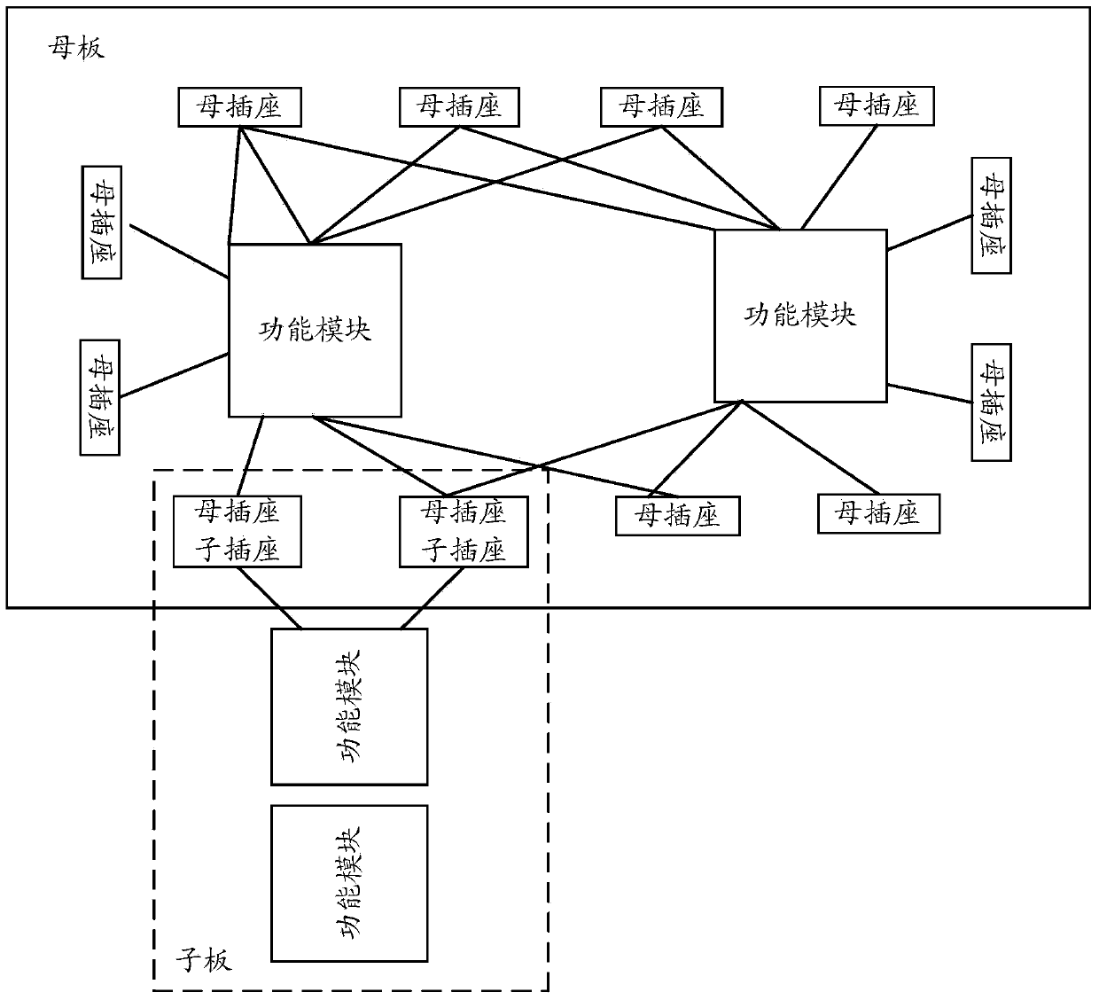
[0061] figure 1 It is a schematic diagram of a motherboard in Embodiment 1 of the present invention, from figure 1 It can be seen that the motherboard includes 2 functional modules, and 12 female sockets are arranged around the 2 functional modules. figure 2 It is a schematic diagram of a daughter board in Embodiment 1 of the present invention, from figure 2 It can be seen that the sub-board includes 2 functional modules, and is provided with 2 sub-sockets. image 3 will be figure 2 The daughter board shown is plugged into the figure 1 shown in the motherboard schematic, image 3 , insert the two sub-sockets on the daughter board into the two female sockets on the motherboard.

[0062] It should be noted, figure 1 motherboard shown and figure 2 The sub-board shown is only used as an example, and the motherboard and the sub-board may also be in other forms in the embodiment of the present invention. Wher...

Embodiment 2

[0083] refer to Figure 5 , which shows a flow chart of a pin mapping method in Embodiment 2 of the present invention, the method may specifically include the following steps:

[0084] Step 501, call the pre-configured script file in the specified directory.

[0085] In the embodiment of the present invention, the script file can be a text TXT file, and the script file is a TXT file configured for the sub-board, and different script files can be configured for different sub-boards according to different requirements, and each script file The names are different. After the script file is configured, it can be saved in a specified directory, and the script file can be searched in the specified directory later, for example, the specified directory can be "F:\HyperSilicon\ProtoWizard-DH\bin". Certainly, the script file may also adopt other file types, and the specified directory may also be another directory, which is not limited in this embodiment of the present invention.

[...

Embodiment 3

[0133] refer to Image 6 , which shows a structural block diagram of a pin mapping device according to Embodiment 3 of the present invention. The device may specifically include the following modules:

[0134] Calling module 601, used to call the pre-configured script file under the specified directory;

[0135] In the embodiment of the present invention, the script file may be a text TXT file.

[0136] The parsing module 602 is configured to parse the script file, the script file includes: the female socket number of the motherboard into which the daughter board is inserted, the daughter socket pin number of the daughter board with a mapping relationship, and the daughter board The pin network name of the functional module on the board;

[0137] A search module 603, configured to search the corresponding pin numbers of the functional modules on the motherboard from a preset database according to the female socket number of the motherboard and the sub-socket pin numbers of t...


PUM


Abstract

The invention provides a pin mapping method and system to solve the problems that, in the prior art, the mapping method is large in working amount and low in efficiency and obtained pin mapping relationships are not accurate. The pin mapping method comprises calling pre-allocated script files under appointed catalogs and analyzing the script files which comprise a number of a main socket into which an auxiliary panel is inserted, a number of an auxiliary socket pin of the auxiliary panel which has a mapping relation and net names of pins of functional modules on the auxiliary panel; searching corresponding main panel number functional module pin numbers in a preset database according to the main socket number of the main panel and the auxiliary socket pin number of the auxiliary panel; integrating into an output file according to the pin net names of the functional modules on the auxiliary panel and the pin numbers of the functional modules on the main panel; outputting the output file. The pin mapping method and system has the advantages of being high in efficiency and accurate in obtained pin mapping relation.

Description

technical field [0001] Embodiments of the present invention relate to the technical field of integrated circuits, and in particular, to a pin mapping method and system. Background technique [0002] An integrated circuit (Integrated Circuit, IC) is a microelectronic device or component. It uses a certain process to interconnect components such as transistors, diodes, resistors, capacitors, and inductors required in a circuit, and interconnects them in a small circuit. One or several small semiconductor wafers or dielectric substrates, and then packaged in a package to become a microstructure with the required circuit functions. With the continuous improvement of user needs, integrated circuits are also constantly developing into large-scale integrated circuits. [0003] In order to improve the versatility of the integrated circuit, the design method of the mother board and the daughter board can be adopted. Among them, the motherboard may include some core function modules...

Claims


Application Information

Patent Timeline
IPC IPC(8): G06F17/50
Inventor 郭文帅刘永宏
Owner 无锡亚科鸿禹电子有限公司
Why Eureka
Try Eureka