Preparation method of transistor with stressed channel and transistor with stressed channel

A technology of strained channels and transistors, which is applied in the direction of transistors, semiconductor/solid-state device manufacturing, semiconductor devices, etc., can solve the problems of high cost, complicated process, difficult strain state of strained materials, etc., and achieve the effect of stable strain and not easy to disappear

Active Publication Date: 2014-04-23
SHANGHAI SIMGUI TECH
View PDF7 Cites 1 Cited by
  • Summary
  • Abstract
  • Description
  • Claims
  • Application Information

AI Technical Summary

Problems solved by technology

However, this method is complex and expensive, and it is difficult for the strained material to maintain a strained state in the subsequent semiconductor planar process and packaging process.

Method used


Image

  • Preparation method of transistor with stressed channel and transistor with stressed channel
  • Preparation method of transistor with stressed channel and transistor with stressed channel
  • Preparation method of transistor with stressed channel and transistor with stressed channel

Examples


Embodiment Construction

[0018] The method for manufacturing a transistor with a strained channel provided by the present invention and the specific implementation of the transistor with a strained channel will be described in detail below in conjunction with the accompanying drawings.

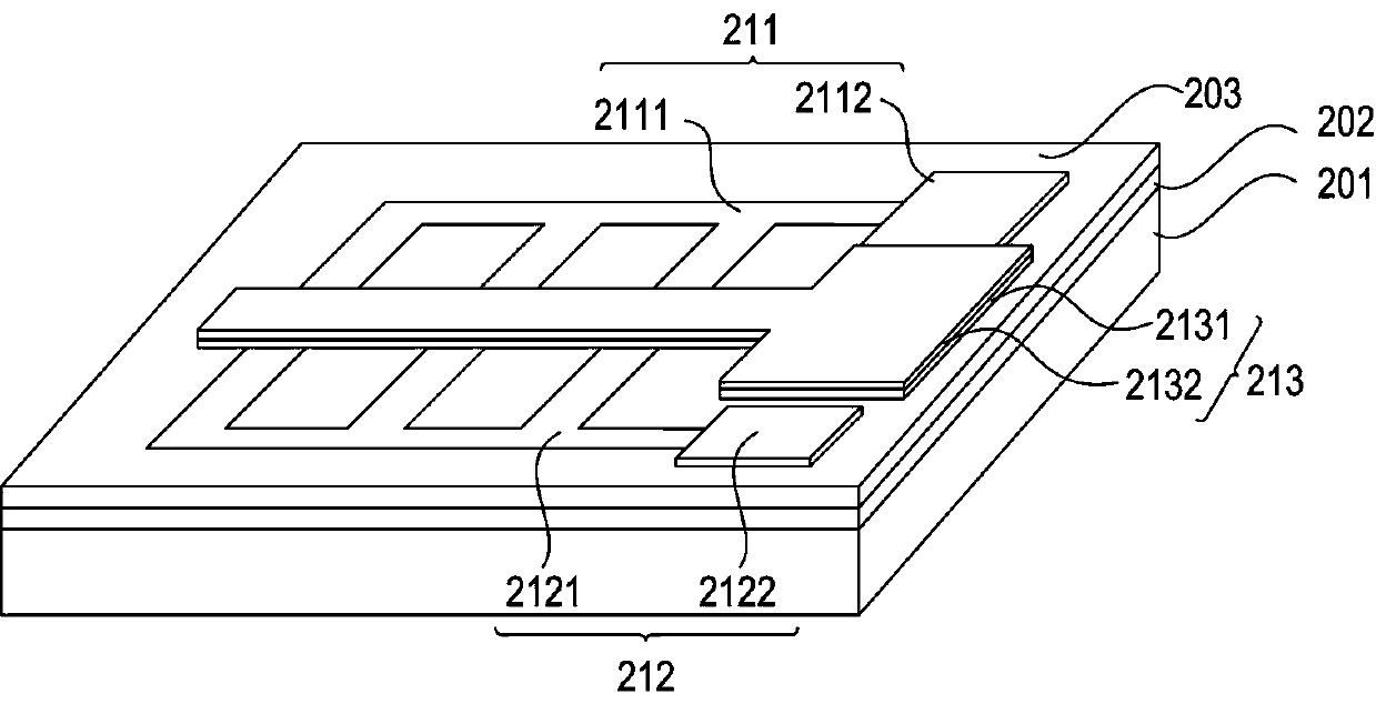
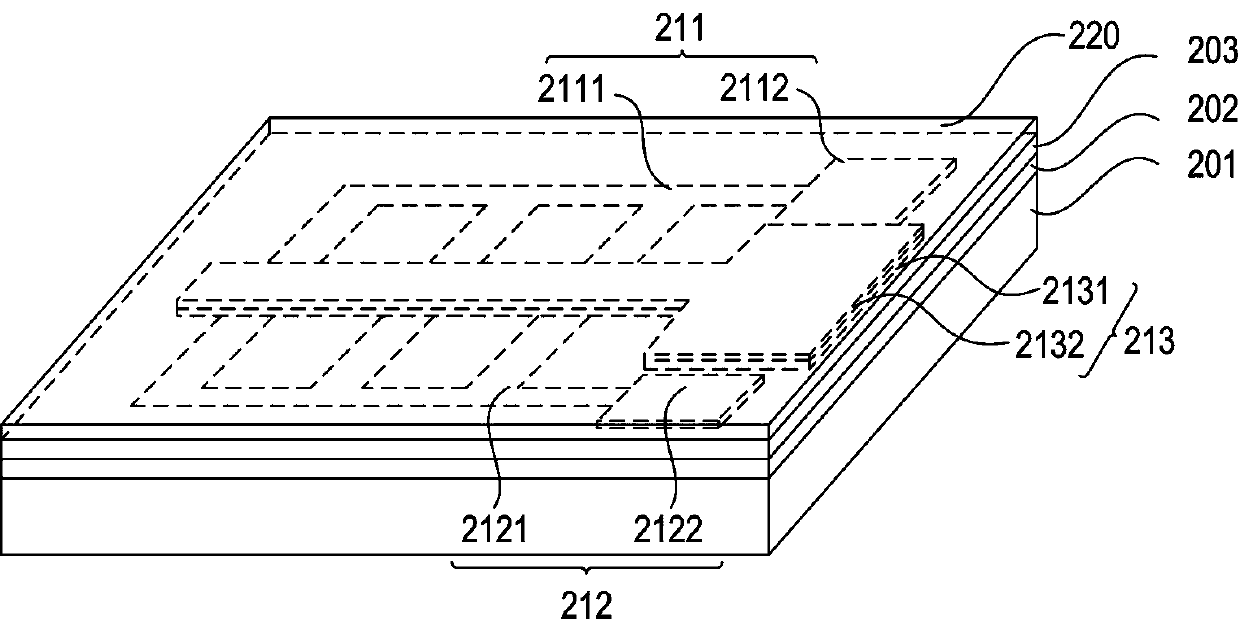
[0019] attached figure 1 Shown is a schematic diagram of the implementation steps of the specific embodiment of the present invention, including: step S10, providing a substrate, the substrate including a support layer, a buried layer on the surface of the support layer, and a device layer on the surface of the buried layer; step S11, forming a transistor, Including forming a source and a drain in the device layer, and forming a gate on the surface of the device layer; Step S12, forming an insulating protection layer on the surface of the device layer, and the insulating protection layer also covers the gate; Step S13, in the A stress layer is formed on the surface of the insulating protection layer, and the stress la...


PUM


Abstract

The invention provides a preparation method of a transistor with a stressed channel and the transistor with the stressed channel. The method comprises the following steps: providing a substrate which comprises a device layer; forming a transistor, including a source electrode and a drain electrode formed in the device layer and a grid electrode formed on the surface of the device layer; forming an insulation protective layer on the surface of the device layer; forming a stress layer on the surface of the insulation protective layer; suspending the device layer where there is a conducting channel of the grid electrode of the transistor such that the device layer is curled under the action of the stress layer, thus leading to tensile strain of the conducting channel of the grid electrode of the transistor. The invention has advantages as follows: the device layer where there is the grid electrode is curled freely and the device layer undergoes strain under the action of the tensile strain; and as the strain is introduced by physical deformation, strain is stable and is not easy to disappear.

Description

technical field [0001] The invention relates to the field of semiconductor devices, in particular to a method for preparing a transistor with a strained channel and a transistor with a strained channel. Background technique [0002] As semiconductor devices shrink in size, traditional bulk silicon materials are approaching their physical limits. However, the requirements for increasing the driving current of MOS devices are getting higher and higher. In order to improve the performance of MOS devices, strained silicon technology has been adopted in the industry to enhance the current driving capability. [0003] The so-called strain technology is a technology that introduces stress at the conductive channel of the MOS device to strain the semiconductor material there, thereby improving the carrier mobility of the conductive channel. Improving the carrier mobility of the conductive channel is beneficial to increasing the driving current of the MOS device. [0004] In the p...

Claims


Application Information

Patent Timeline
Patent Type & Authority Applications(China)
IPC IPC(8): H01L21/336H01L29/78H01L29/10
CPCH01L29/1033H01L29/66568H01L29/7845
Inventor 魏星母志强薛忠营狄增峰方子韦
Owner SHANGHAI SIMGUI TECH
Why Eureka
Try Eureka