Readout circuit and nonvolatile memory using same
A readout circuit, non-volatile technology, applied in read-only memory, static memory, digital memory information and other directions, can solve the problems of amplifier gain decrease, increase of readout circuit malfunction, and readout circuit function stop.
- Summary
- Abstract
- Description
- Claims
- Application Information
AI Technical Summary
Problems solved by technology
Method used
Image
Examples
Embodiment 1
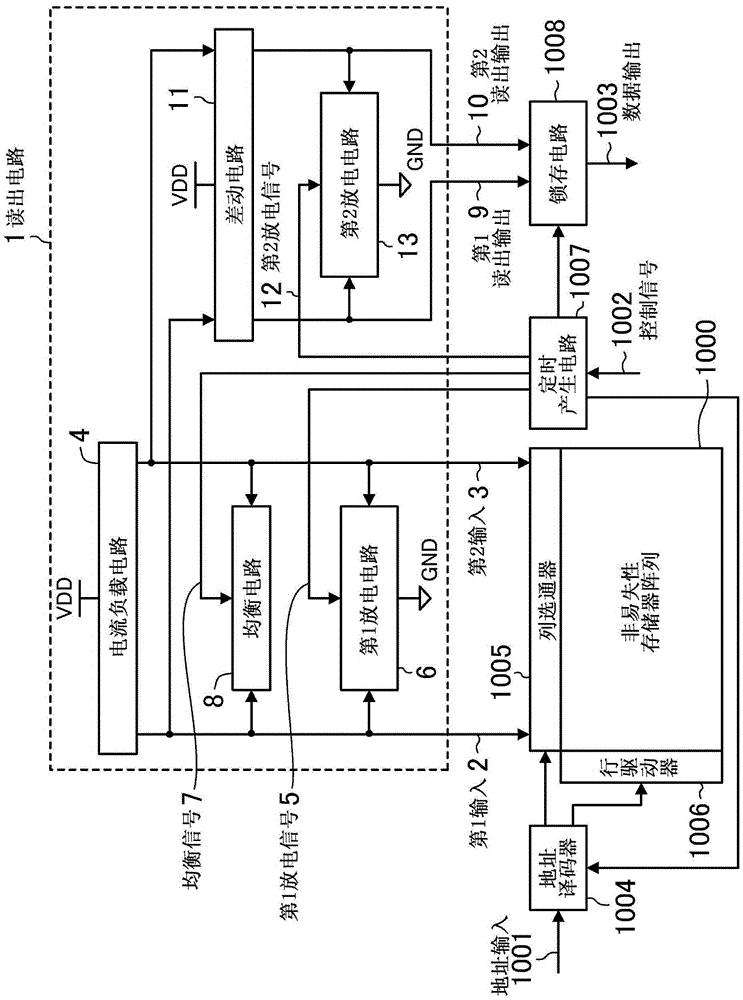
[0112] First, the readout circuit according to Embodiment 1 will be described.
[0113] figure 1 It is a block diagram of a nonvolatile memory including a readout circuit as an embodiment of the present invention. The first input 2 and the second input 3 of the readout circuit 1 are connected to the nonvolatile memory array 1000 through a column gate 1005 . The first input 2 and the second input 3 are respectively connected to a nonvolatile memory cell (sometimes simply referred to as a memory cell) or a reference cell included in the nonvolatile memory array 1000 .
[0114] It is assumed that the reference cell uses a nonvolatile memory cell similarly to the memory cell, or replaces the variable resistance element of the memory cell with a polysilicon resistor, a transistor, or the like. In addition, the reference cell is not limited to these configurations as long as it serves as a reference for comparison of the memory cells. The readout circuit 1 outputs a differential ...
Embodiment 2
[0132] Next, the readout circuit according to the second embodiment will be described using a transistor-level equivalent circuit.
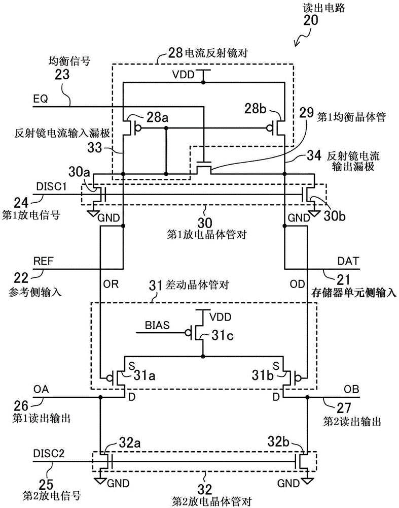
[0133] figure 2 It is a circuit diagram of the readout circuit according to the second embodiment, and specifically shows the configuration of the first embodiment using transistors.
[0134] The readout circuit 20 consists of a current mirror pair 28 with a pair of P-channel transistors 28a, 28b, a first equalization transistor 29, a first discharge transistor pair 30 with a pair of N-channel transistors 30a, 30b, and a pair of P-channel transistors. A differential transistor pair 31 of channel transistors 31a and 31b and a second discharge transistor pair 32 having a pair of N channel transistors 32a and 32b are constituted.
[0135] The mirror current input drain 33 of the current mirror pair 28 is connected to the reference side input 22 (REF), and the mirror current output drain 34 is connected to the memory cell side input 21 (DAT). The ...
Embodiment 3
[0148] Next, as a third embodiment, a readout circuit in which a clamp transistor pair is added to the configuration of the second embodiment will be described. Figure 4 It is a circuit diagram of the readout circuit according to the third embodiment, and is an equivalent circuit diagram of the readout circuit shown in the first embodiment.
[0149] Readout circuit 300 includes clamp transistor pair 36 having a pair of N-channel transistors 36a, 36b. A clamp transistor pair 36 is inserted into the reference side input 22, the memory cell side input 21, respectively. Specifically, the mirror current input drain 33 is connected to the reference side input 22 via the drain and source of the N-channel transistor 36a. The mirror current output drain 34 is connected to the memory cell side input 21 via the drain and source of the N-channel transistor 36b. The respective gates of the N-channel transistors 36a, 36b are commonly connected to the clamp voltage input 35 . The clamp t...
PUM
 Abstract
Description
Claims
Application Information


