
Design method and system for quickly generating light painting layer of printed circuit board (PCB)

A level, light painting technology, applied in the electronic field, can solve problems such as time-consuming and energy-consuming, time-wasting, and error-prone, and achieve the effects of saving time, improving accuracy, and quickly generating

Inactive Publication Date: 2014-05-07
INSPUR BEIJING ELECTRONICS INFORMATION IND
View PDF0 Cites 5 Cited by
  • Summary
  • Abstract
  • Description
  • Claims
  • Application Information

AI Technical Summary

Problems solved by technology

[0002] At present, we use Cadence Allegro software for PCB design. It is cumbersome to add some information such as layering and light painting, and it takes a lot of time and energy. Usually, we add relevant information manually, or export layers from other boards, and then import them. In the new PCB, you need to carefully confirm the relevant information
The above approach is not only a waste of time, but also prone to errors. In view of this situation, there is an urgent need for a tool that can quickly and accurately generate relevant information

Method used


Image

  • Design method and system for quickly generating light painting layer of printed circuit board (PCB)
  • Design method and system for quickly generating light painting layer of printed circuit board (PCB)
  • Design method and system for quickly generating light painting layer of printed circuit board (PCB)

Examples


Embodiment Construction

[0016] Hereinafter, the present invention will be described in detail with reference to the drawings and examples. It should be noted that, in the case of no conflict, the embodiments in the present application and the features in the embodiments can be combined with each other.

[0017] The invention provides a design method for quickly generating PCB light-drawing layers, comprising the following steps:

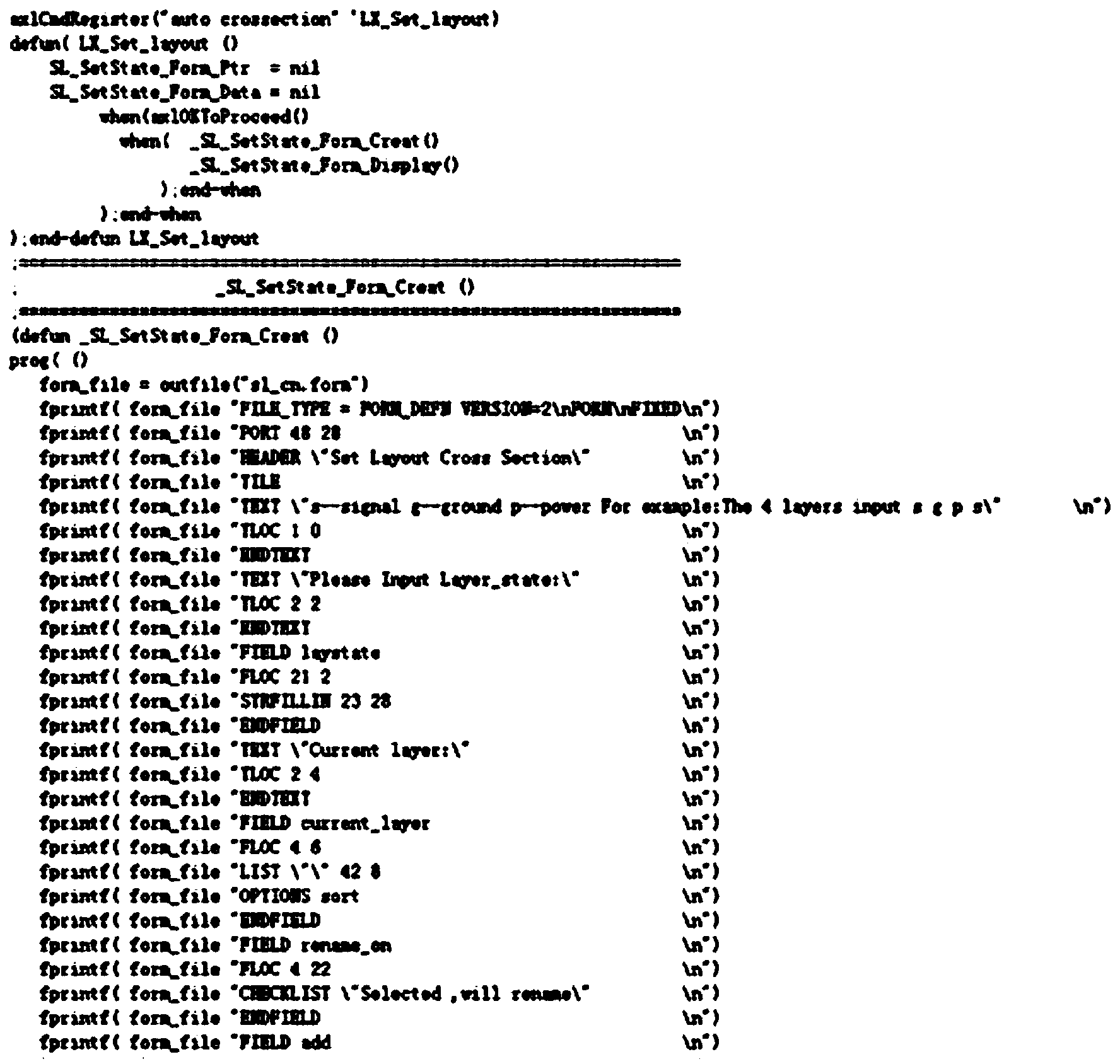
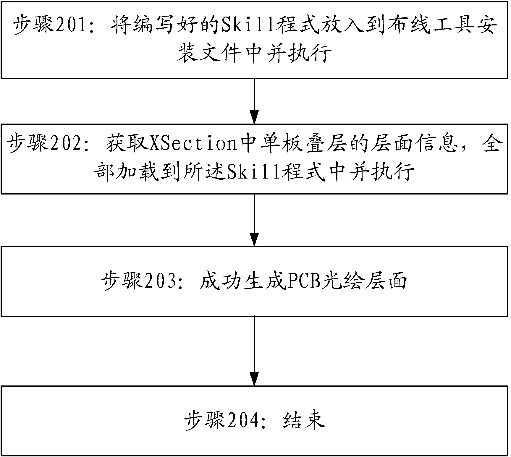
[0018] Put the written Skill program into the wiring tool installation file and execute it;

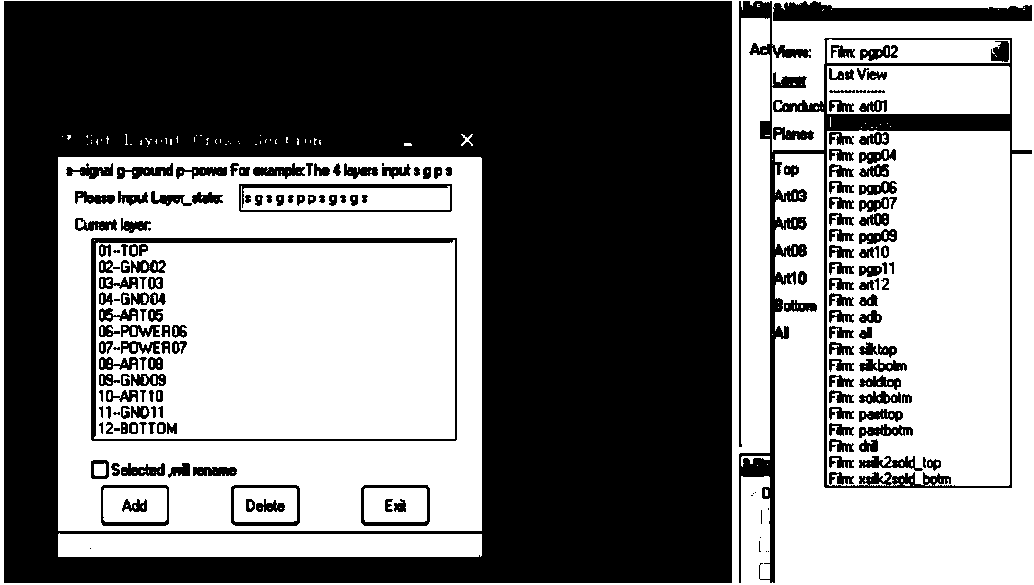
[0019] Load the layer information of the single board stack and execute it to generate the PCB light drawing layer.

[0020] Wherein, the process of inputting and executing the level information of the single board stack is:

[0021] Obtain the layer information of the veneer stack in XSection, load all of them into the Skill program and execute it.

[0022] Among them, the way to load all the layer information of the veneer stack in the XSection into the Skill program is as fol...


PUM


Abstract

The invention provides a design method and a design system for quickly generating a light painting layer of a printed circuit board (PCB), which are applied to the field of electronics. The method comprises the following steps of putting a written Skill program into a wiring tool installation file and executing; loading veneer laminated layer information and executing to generate the light painting layer of the PCB. By the method and the system, the manually added light painting layer information of the PCB is converted into automatically quickly generated light painting layer information; by the design method, the light painting layer information in the PCB is quickly generated, so that time is shortened and the accuracy of the layer is improved.

Description

technical field [0001] The invention relates to the field of electronics, in particular to a design method and system for rapidly generating PCB light-drawing layers. Background technique [0002] At present, we use Cadence Allegro software for PCB design. It is cumbersome to add some information such as layering and light painting, and it takes a lot of time and energy. Usually, we add relevant information manually, or export layers from other boards, and then import them. In the new PCB, the relevant information needs to be carefully confirmed at the end. The above approach not only wastes time, but is also prone to errors. In view of this situation, there is an urgent need for a tool that can quickly and accurately generate relevant information. Contents of the invention [0003] The present invention provides a design method and system for quickly generating PCB light-drawing layers to solve the above problems. [0004] The invention provides a design method for quic...

Claims


Application Information

Patent Timeline
Patent Type & Authority Applications(China)
IPC IPC(8): G06F17/50
Inventor 胡立燕赵亚民李鹏翀
Owner INSPUR BEIJING ELECTRONICS INFORMATION IND
Learn More