Array substrate and display device

A technology of array substrates and adjacent columns, applied in nonlinear optics, instruments, optics, etc., can solve the problems of increasing the wiring around AA, increasing the shielding width of data lines, and increasing the space of fan-out areas, etc. Achieve the effect of ultra-narrow bezel design, reduce wiring space, and reduce shielding width

Inactive Publication Date: 2014-05-14
BEIJING BOE DISPLAY TECH CO LTD +1
View PDF5 Cites 15 Cited by
  • Summary
  • Abstract
  • Description
  • Claims
  • Application Information

AI Technical Summary

Problems solved by technology

[0005] The inventors found that there are at least the following problems in the prior art: due to the doubling of the number of data lines, the black matrix (BM) shading width on the side of the data lines increases, thereby reducing the pixel aperture ratio, which in turn causes an increase in optical costs, such as figure 2 shown
Moreover, for ultra-narrow bezel display, it is necessary to minimize the size around the effective display area (AA, active area), which increases the difficulty of wiring around AA
At this time, since the number of data lines doubles, the space required for the fan-out area (Fan-out wiring area) will also increase accordingly.

Method used


Image

  • Array substrate and display device
  • Array substrate and display device
  • Array substrate and display device

Examples


Embodiment 1

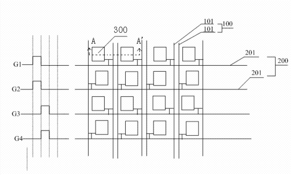
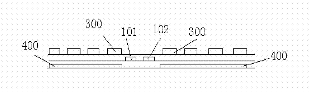
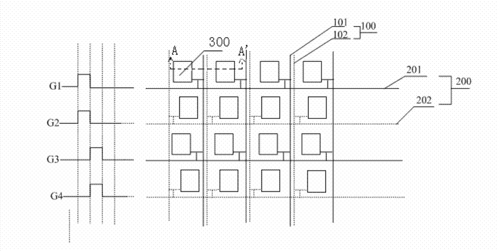
[0027] like Figure 3-6 As shown, this embodiment provides an array substrate, which includes multiple sets of data lines 100 and multiple sets of gate lines 200 arranged crosswise, and a set of data lines 100 is arranged between pixel units in two adjacent columns, and each set of data lines The line 100 includes a first data line 101 and a second data line 102, each group of gate lines 200 includes a first gate line 201 and a second gate line 202, at the intersection of the first gate line 201 and the first data line 101, and A pixel unit is defined at the intersection of the second gate line 202 and the second data line 102, wherein the first data line 101 of each group of data lines 100 is arranged in the first data line layer, and the second data line 102 It is arranged on the second data line layer, and the projections of the first data line 101 and the second data line 102 on the array substrate do not overlap.

[0028] The first data lines 101 and the second data line...

Embodiment 2

[0042] This embodiment provides a display device, which includes the array substrate described in Embodiment 1. The display device may be any product or component with a display function such as a mobile phone, a tablet computer, a television, a monitor, a notebook computer, a digital photo frame, a navigator, and the like.

[0043] Since the display device of this embodiment includes the array substrate described in Embodiment 1, its frame is narrow and its aperture ratio is high.

[0044] Of course, the display device of this embodiment may also include other conventional structures, such as a display driving unit and the like.


PUM


Abstract

The invention provides an array substrate and a display device, and belongs to the technical field of display. The array substrate and the display device can solve the problem that an existing display device is low in resolution. The array substrate comprises multiple sets of data lines and multiple sets of grid lines, wherein the data lines and the grid lines are ranked in an intersecting mode, one set of data lines are arranged between every two adjacent pixel units, each set of data lines comprise the first data line and the second data line, each set of grid lines comprise the first grid line and the second grid line, and the pixel units are limited at the intersections of the first grid lines and the first data lines and the intersections of the second grid lines and the second data lines. The first data line in each set of data lines is arranged on a first data line layer, the second data line in each set of data lines is arranged on a second data line layer, and the projection of the first data line and the projection of the second data line on the array substrate do not coincide. The display device comprises the array substrate.

Description

technical field [0001] The invention belongs to the field of display technology, and in particular relates to an array substrate and a display device. Background technique [0002] Thin Film Transistor Liquid Crystal Display (TFT-LCD for short) is a main flat panel display (Flat Panel Display, FPD for short). It has become a mainstream product in the market. [0003] Currently in the TFT-LCD industry, display devices with ultra-high-definition and ultra-narrow bezels have become the technological development trend of enterprises. Especially for large-sized display panels, for example, a resolution of 4K*2K, or even a resolution of 8K*4K has become the mainstream in the market. However, in order to increase the resolution, the first technical problem to be overcome is the guarantee of pixel charging ratio. Since the resolution is positively correlated with the number of pixel units per unit area, the higher the resolution of the display panel, the more the number of pixel ...

Claims


Application Information

Patent Timeline
Patent Type & Authority Applications(China)
IPC IPC(8): G02F1/1362G02F1/13
Inventor 高玉杰朴相镇
Owner BEIJING BOE DISPLAY TECH CO LTD
Why Eureka
Try Eureka