Bidirectional IGBT device and manufacturing method thereof

A device and source region technology, which is applied in semiconductor/solid-state device manufacturing, semiconductor devices, electrical components, etc., can solve the problems of drift region thick drift region, depletion layer cannot penetrate, poor performance, etc., and achieve good carrier Concentration distribution and electric field distribution, good forward conduction characteristics, effect of thin drift region thickness

Inactive Publication Date: 2014-05-14
UNIV OF ELECTRONICS SCI & TECH OF CHINA
View PDF4 Cites 25 Cited by
  • Summary
  • Abstract
  • Description
  • Claims
  • Application Information

AI Technical Summary

Problems solved by technology

[0005] The present invention provides a bidirectional IGBT device and a manufacturing method thereof aiming at the technical problems that the depletion layer cannot pass through the drift region when the device is blocked, the drift region is thick and the performance is poor in the existing bidirectional IGBT device.

Method used


Image

  • Bidirectional IGBT device and manufacturing method thereof
  • Bidirectional IGBT device and manufacturing method thereof
  • Bidirectional IGBT device and manufacturing method thereof

Examples


Embodiment Construction

[0047] Below in conjunction with accompanying drawing, describe technical scheme of the present invention in detail:

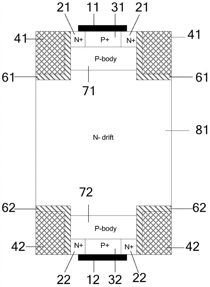
[0048] Such as figure 2 As shown, it is a schematic diagram of the bidirectional IGBT structure of the present invention, and its cell structure includes two MOS structures symmetrically arranged on the front and back sides of the substrate drift region; Two N+ source regions 21 or 22 in the body region 71 or 72, one P+ body contact region 31 or 32 disposed in the P-type body region 71 or 72 and located in the middle of the two N+ source regions 21 or 22; Each N+ source region 21 or 22 and the surface of the P+ body contact region 31 or 32 are connected to the metal electrode 11 or 12; the N-channel MOS structure also includes two identical gate structures, and the gate structure is a trench The gate structure is composed of a trench wall gate dielectric 61 or 62 and a trench inner gate conductive material 41 or 42, wherein a side part of the trench gate die...


PUM


Abstract

The invention belongs to the technical field of power semiconductor devices and provides a bidirectional IGBT device and manufacturing method thereof. The cellular structure of the bidirectional IGBT device comprises two MOS structures symmetrically arranged on the front face and the back face of a substrate drift region, N-shaped buried layers are arranged between P-shaped body areas of the MOS structures and the substrate drift region, and P-shaped buried layers are arranged between the bottom of grid structures of MOS structures and the substrate drift region. The bidirectional IGBT device can be formed by respectively manufacturing two silicon wafers and bonding the silicon wafers, and also can be formed by processing the double faces of a single wafer. According to the bidirectional IGBT device and manufacturing method of the bidirectional IGBT device, an IGBT has good symmetrical positive and reverse characteristics and has a thinner drift region thickness, better carrier concentration distribution and electric field distribution under the same device withstand voltage, so that the device obtains the trade-off of a better positive conductive characteristic, a positive conductive characteristic and a turn-off loss characteristic.

Description

technical field [0001] The invention belongs to the technical field of power semiconductor devices, and relates to a bidirectional insulated gate bipolar transistor (Bi-directional IGBT) and a manufacturing method thereof. Background technique [0002] Insulated gate bipolar transistor (IGBT) is a new type of power electronic device combining MOS field effect and bipolar transistor. It not only has the advantages of easy driving and simple control of MOSFET, but also has the advantages of low conduction voltage of power transistor, large on-state current and small loss. It has become one of the core electronic components in modern power electronic circuits and is widely used in Various fields of the national economy such as communications, energy, transportation, industry, medicine, household appliances and aerospace. The application of IGBT plays an extremely important role in improving the performance of power electronic systems. [0003] In a traditional AC-DC-AC conver...

Claims


Application Information

Patent Timeline
Patent Type & Authority Applications(China)
IPC IPC(8): H01L29/739H01L29/06H01L21/331
CPCH01L21/187H01L29/0603H01L29/66325H01L29/7393
Inventor 张金平杨文韬单亚东顾鸿鸣刘竞秀李泽宏任敏张波
Owner UNIV OF ELECTRONICS SCI & TECH OF CHINA
Why Eureka
Try Eureka