Check patentability & draft patents in minutes with Patsnap Eureka AI!

A kind of support device of semiconductor wafer

A supporting device and semiconductor technology, which is applied in semiconductor/solid-state device manufacturing, electrical components, circuits, etc., can solve the problems of increased equipment cost, complex support ring structure, and increased processing difficulty, so as to reduce the occupied area and crystal Circle breakage rate, the effect of reducing the generation of particles

Active Publication Date: 2016-04-06
BEIJING SEVENSTAR ELECTRONICS CO LTD
View PDF5 Cites 0 Cited by
  • Summary
  • Abstract
  • Description
  • Claims
  • Application Information

AI Technical Summary

Problems solved by technology

Although the design form of this device can easily meet the hand space of the manipulator by adjusting the position of the supporting feet on the circumference of the supporting ring, so as to facilitate the operation of the manipulator, there are also obvious problems at the same time: this supporting foot device is due to the wafer support of the supporting feet. The support surface is located at the front end of the support leg, and the assembly position with the support ring is located at the rear end of the support leg, so that the inner diameter of the support ring is larger than the outer diameter of the wafer, and the outer diameter of the support ring exposes a lot of the outer diameter of the wafer
Moreover, the structure of the support ring of the device is also relatively complicated, which greatly increases the difficulty of processing and increases the cost of equipment.

Method used


Image

  • A kind of support device of semiconductor wafer
  • A kind of support device of semiconductor wafer
  • A kind of support device of semiconductor wafer

Examples


Embodiment 1

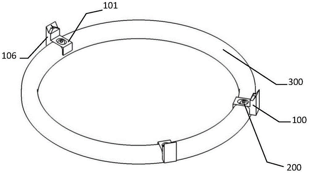
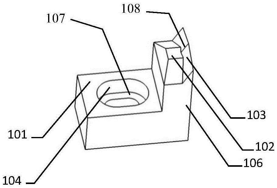
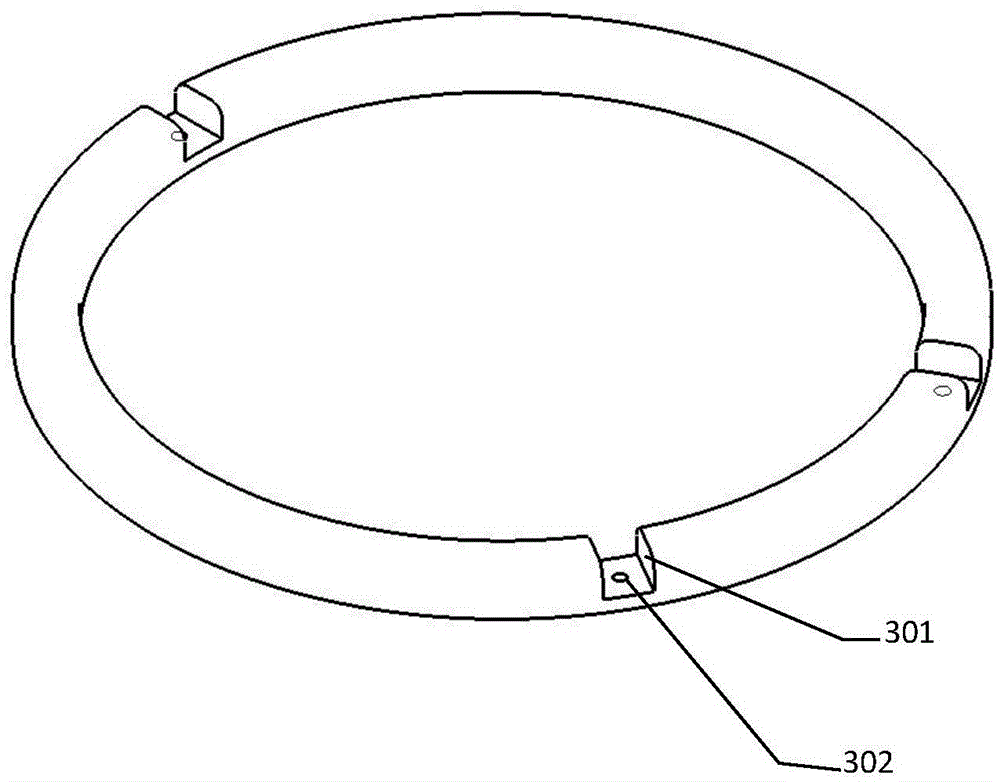
[0028] In this example, see figure 1 , figure 1 It is a schematic diagram of the assembly structure of a semiconductor wafer support device of the present invention. As shown in the figure, the support device for the wafer of the present invention includes an annular support ring 300 installed on the upper end of the wafer storage table (omitted in the figure) in the wafer transfer system of the semiconductor process equipment, and a support wafer installed on the circumference of the support ring The 3 supporting feet 100. The supporting legs are L-shaped, and the upper end of the L-shaped vertical part 106 is provided with a wafer support surface, and the L-shaped horizontal part 101 is processed with a waist-shaped hole, and a mounting step is processed in the waist-shaped hole, and the screw 200 passes through the waist-shaped hole , and securely connect the support foot with the support ring through the installation step. The support foot is installed and connected wit...

Embodiment 2

[0038] In this example, see Figure 5 , Figure 5 It is another structural schematic diagram of the supporting foot of a semiconductor wafer supporting device of the present invention. As shown in the figure, the shape of the supporting foot is still L-shaped, and the structure of the L-shaped horizontal part 101 is consistent with the supporting foot exemplified in the first embodiment. In this embodiment, the upper end of the L-shaped vertical portion 106 of the support leg is provided with a wafer support surface, and the wafer support surface is composed of two intersecting downwardly inclined wafer support surfaces 105 . The apexes 110 of the two intersecting downward inclined surfaces coincide with the axisymmetric central planes of the supporting legs, that is, they are located in the center. In this way, the contact area between the wafer and the wafer supporting surface can be reduced, and the utilization rate of the wafer can be improved. The two intersecting slop...


PUM


Abstract

The invention discloses a support device of a semiconductor wafer. The support device of the semiconductor wafer comprises an annular support ring and a plurality of supporting legs, wherein the annular support ring is mounted at the upper end of a wafer storage table in a wafer transferring system of semiconductor process equipment, and the supporting legs are mounted on the circumference of the support ring for supporting the wafer. Each supporting leg is L-shaped, a wafer support surface is mounted at the upper end of the vertical part of the L shape, the horizontal part of the L shape is connected with the support ring, and the supporting leg is connected with the support ring in the mode that the vertical part of the L shape is located at the outer side and the horizontal part is located at the inner side. The support ring of the support device of the semiconductor wafer is reduced in volume, and accordingly the floor space of the equipment is reduced, the wafer is avoided from breaking due to falling to the ground from the inner diameter of the support ring, the wafer is easier to put stably, the damage caused by friction and the particle generation are reduced, and the support device of the semiconductor wafer is applicable to be popularized in factories.

Description

technical field [0001] The present invention relates to a wafer storage table in a semiconductor process equipment wafer transfer system, and more particularly, to a wafer support device for a wafer storage table in a semiconductor process equipment wafer transfer system. Background technique [0002] Semiconductor manufacturing is a series of cycles and repetitions of major process steps. Many fabrication processes involve chemical reactions that take place within the process chamber of semiconductor process equipment. Today, the processing of semiconductor wafers usually involves chemical reactions that take place in process chambers. [0003] According to different processing processes, wafers often need to be transported between process chambers of multiple semiconductor process equipment through a wafer transfer system. In the process equipment, the main function of the wafer transfer system is to load the wafers, and all loading and unloading are done by automatic ma...

Claims


Application Information

Patent Timeline
Patent Type & Authority Patents(China)
IPC IPC(8): H01L21/687
CPCH01L21/68785
Inventor 李广义赵宏宇
Owner BEIJING SEVENSTAR ELECTRONICS CO LTD
Features
  • R&D
  • Intellectual Property
  • Life Sciences
  • Materials
  • Tech Scout
  • Unparalleled Data Quality
  • Higher Quality Content
  • 60% Fewer Hallucinations
Learn More