Method for forming photo composition

A patterning and line patterning technique used in the field of forming nanoscale structures

Active Publication Date: 2014-06-04
IBM CORP
View PDF5 Cites 18 Cited by
  • Summary
  • Abstract
  • Description
  • Claims
  • Application Information

AI Technical Summary

Problems solved by technology

However, lithographic alignment of the cut pattern produced using the cut mask to the pre-existing pattern is a challenge

Method used


Image

  • Method for forming photo composition
  • Method for forming photo composition
  • Method for forming photo composition

Examples


Embodiment Construction

[0049] As described above, the present disclosure relates to a method of forming a nanoscale structure, and more particularly, to a method of forming a nanoscale fin structure cut perpendicular to a length direction, and a structure for forming the nanoscale fin structure. Aspects of the present disclosure will now be described in detail using the accompanying drawings. It should be noted that identical and corresponding elements are denoted by the same reference numerals.

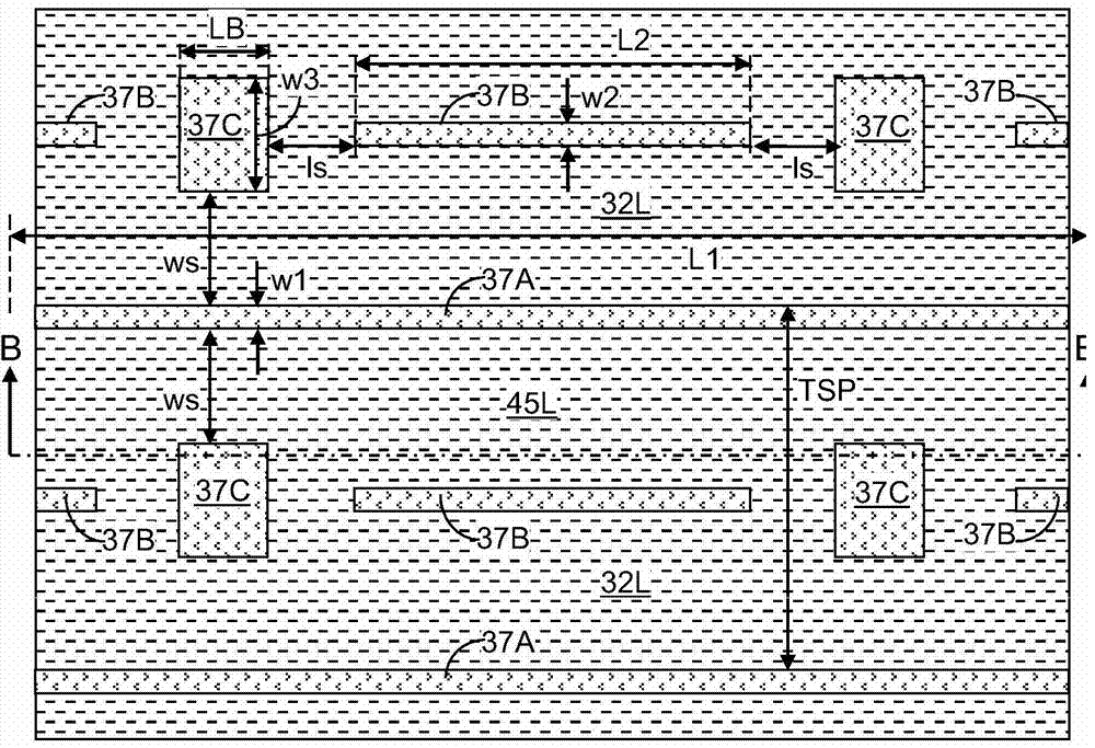
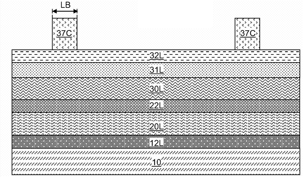
[0050] refer to Figure 1A and 1B , the first exemplary patterning structure according to an embodiment of the present disclosure includes a material stack formed over the substrate 10 . The material stack may include, from bottom to top, a first material layer 12L, an underlying organic planarization layer (OPL) 20L, a second material layer 22L, an organic planarization layer (OPL) 30L, a hard mask layer 31L and Neutral polymer layer 32L. Subsequently, a patterned template layer ( 37A, 37B, 37C) is for...


PUM

PropertyMeasurementUnit
thicknessaaaaaaaaaa
surface roughnessaaaaaaaaaa

Abstract

The invention relates to a method for forming a photo composition; a mold plate layer is formed on a neutral polymer layer, and self-assembling segmented copolymer material is applied and automatically assembled; the mold plate layer comprises a first linear portion, a second linear portion shorter than the first linear portion, and a block-shaped mold plate structure with the width bigger than the second linear portion; in a zone far away from a portion extending in the width direction, the self-assembling segmented copolymer material is arranged in an alternate thin layer through phase separation; the block-shaped mold plate structure disturbs the thin layer and causes the thin layer to stop; when the copolymer segmented content is selectively removed, a cavity parallel to the first and second linear portions is formed, and the cavity can stop with the block-shaped mole plate structure in an autocollimation manner; the graph of the cavity can be reverted and transferred to the material layer so as to form fins with different lengths.

Description

[0001] Statement Regarding Federally Sponsored Research or Development [0002] This invention was made with Government support under Contract No. FA8650-10-C-7038 awarded by the Defense Advanced Research Projects Agency (DARPA). The government has certain rights in this invention. technical field [0003] The present disclosure generally relates to methods of forming nanoscale structures, and more particularly to methods of forming nanoscale fin structures cut perpendicular to a length direction and structures for forming the nanoscale fin structures. Background technique [0004] Fin structures that extend lengthwise with a uniform width are useful in semiconductor fabrication. For example, semiconductor fins may be used to form fin field effect transistors that employ the sidewalls of the semiconductor fin as the channel of the transistor. [0005] Fins may be formed by patterning a material layer, such as a semiconductor material layer, using an etch mask and an anisot...

Claims


Application Information

Patent Timeline
Patent Type & Authority Applications(China)
IPC IPC(8): H01L21/20H01L29/06H01L29/78H01L21/336
CPCH01L29/66803H01L29/785H01L21/3086H01L21/0337G03F7/0002G03F7/165G03F7/0035B81B7/0006B81B2203/0353B81B2207/07B81C1/00031B81C2201/0149B81C2201/0198H01L21/31144
Inventor M·A·古罗恩黎家辉J·W·皮特拉蔡欣妤
Owner IBM CORP
Why Eureka
Try Eureka