Adjustment method for parameters of chips on wafer

A chip and parameter technology, which is applied in the field of chip parameter adjustment on the wafer, can solve the problems of increased test time, inability to meet mass production, and different chips, and achieve the effect of shortening the test time

Active Publication Date: 2014-06-11
SHANGHAI HUAHONG GRACE SEMICON MFG CORP
View PDF6 Cites 21 Cited by
  • Summary
  • Abstract
  • Description
  • Claims
  • Application Information

AI Technical Summary

Problems solved by technology

[0004] However, when large-scale logic testing instruments test chips, from the perspective of production, they often use large-scale simultaneous testing, and cannot apply different trimming values ​​to each chip, resulting in the accuracy of trimming in mass production. too low
In order to improve the accuracy of trimming, the parameters of each chip can only be trimmed separately, which will lead to a multiplied increase in test time and cannot meet the needs of mass production

Method used


Image

  • Adjustment method for parameters of chips on wafer
  • Adjustment method for parameters of chips on wafer
  • Adjustment method for parameters of chips on wafer

Examples


Embodiment Construction

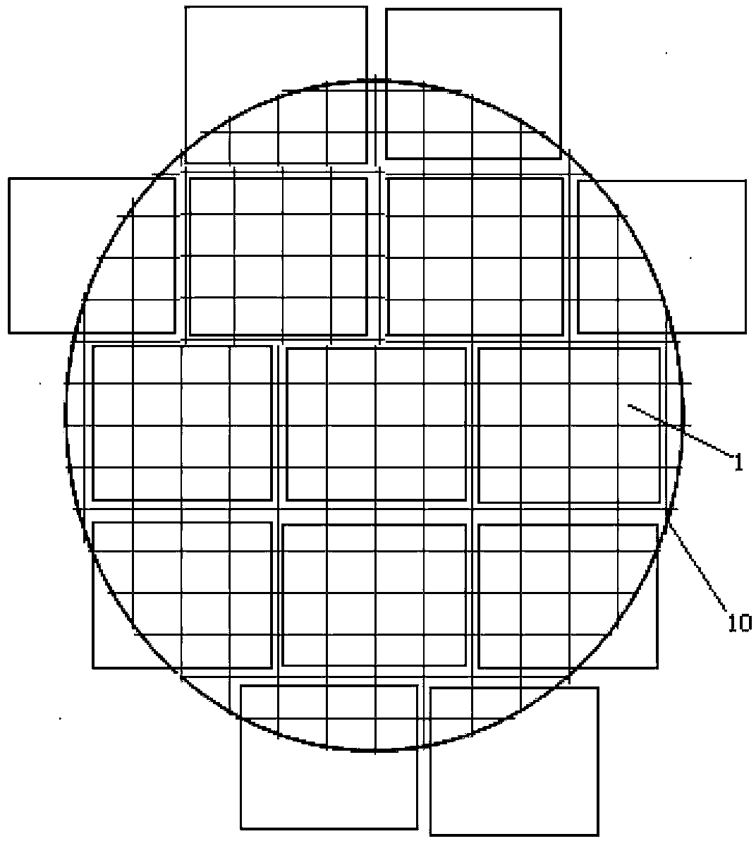
[0030] Such as figure 1 As shown, the trimming method of chip parameters on the wafer of the present invention comprises the following steps:

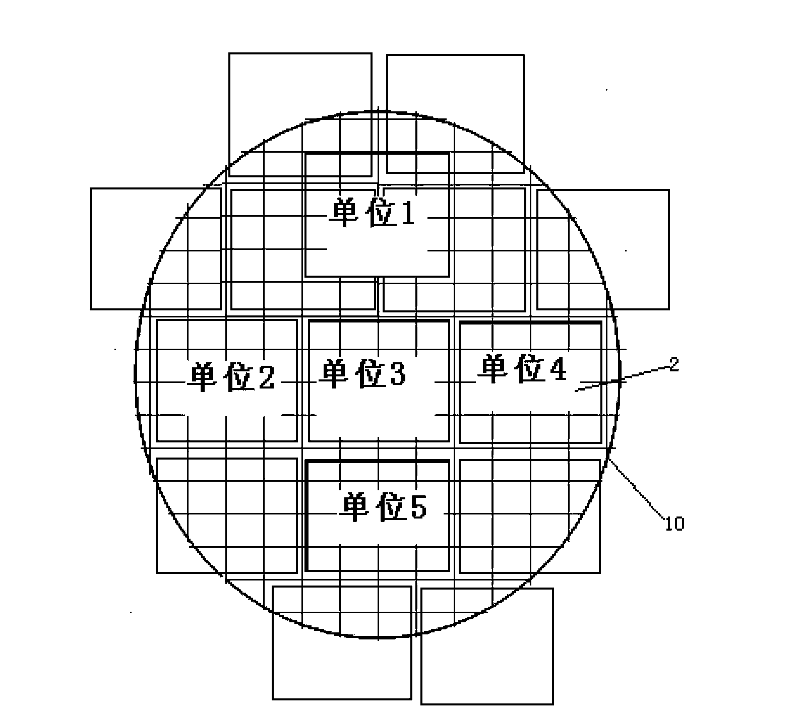
[0031] In the first step, all the chips on the test wafer 10 are divided into multiple test units ( figure 1 divided into 14 test units1);

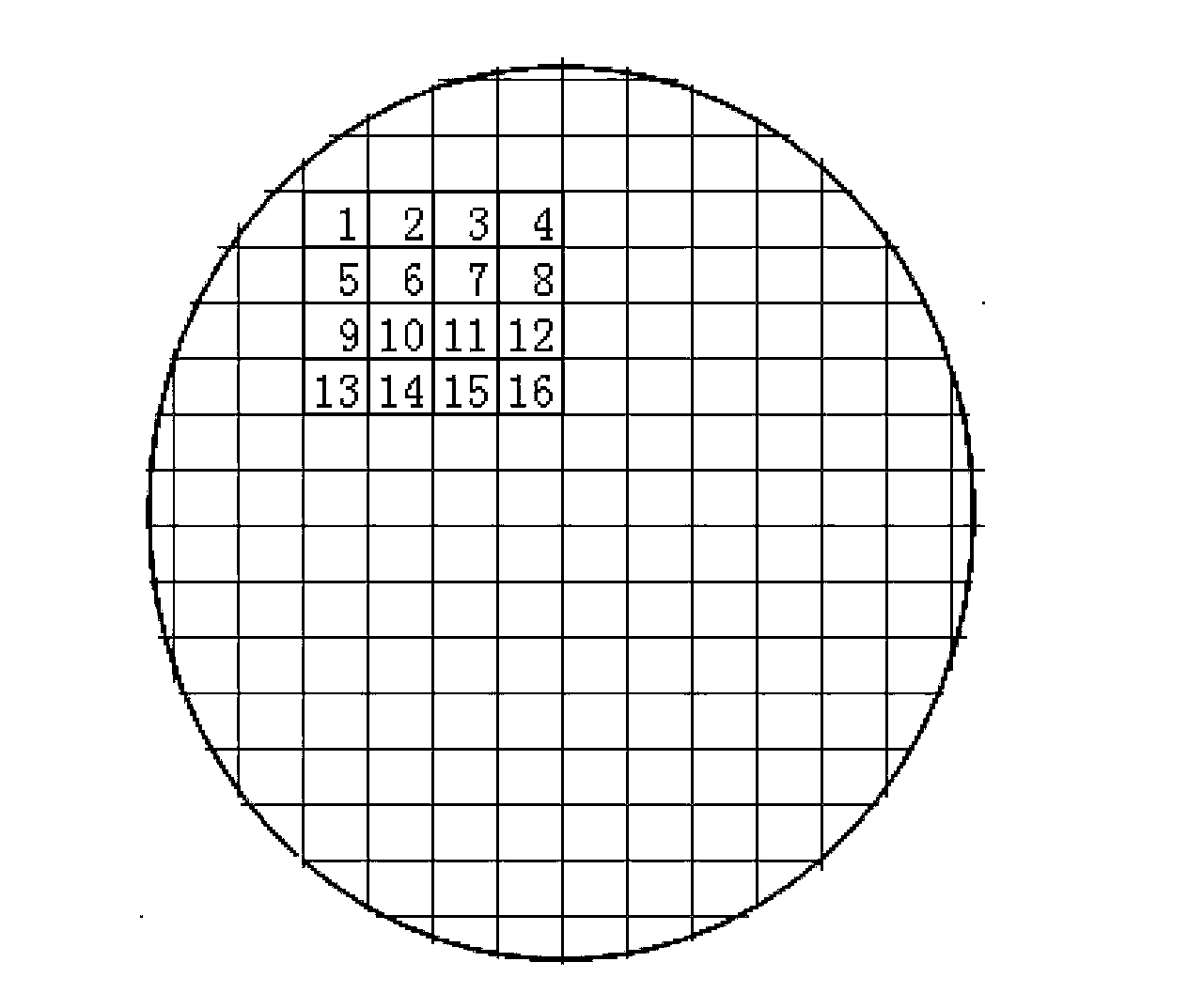
[0032] Such as figure 2 As shown, if the probe card can pierce 16 chips at a time, each test unit contains a maximum of 16 chips, so that the probe card can measure the parameter eigenvalues ​​of all chips in the test unit every time;

[0033] The second step is to measure a parameter that needs to be adjusted by each chip in a test unit through the probe card, and obtain the eigenvalue of the parameter of all chips in the test unit;

[0034] The parameters of the chip can be the reference voltage value of the chip, the functional voltage value of the chip, the current value of the chip, and the frequency of the chip;

[0035] The third step is to take the average value of the parameter eigen...


PUM


Abstract

The invention discloses an adjustment method for parameters of chips on a wafer. The method includes the following steps: step1: grouping all chips on a test wafer into a plurality of test units; step2: measuring a specific parameter of each chip in a specific test unit through a probe card so as to obtain eigenvalues of the parameters of all the chips in the test unit; step3: obtaining a mean value of the eigenvalues of the parameters of all the chips in the test unit and using the mean value of the parameters as an adjustment target value of all the chips in the test unit and at the same time writing the mean value of the parameters into the chips for being used in follow-up tests and normal work so as to complete adjustment of a specific test unit on the test wafer; step4: repeating the step 2 and step3 until adjustment of all test units on the test wafer is completed. The adjustment method for the parameters of the chips on the wafer is capable of ensuring the adjustment accuracy while ensuring large-scale mass production.

Description

technical field [0001] The invention relates to a test method for large-scale integrated circuits, in particular to a method for adjusting chip parameters on a wafer. Background technique [0002] When large-scale integrated circuits are tested, some parameters of the chip often need to be adjusted. Each chip may have many different parameters that need to be adjusted, such as including the chip's reference voltage value, chip's functional voltage value, chip's current value, and chip frequency. Due to production reasons, the eigenvalues ​​of these parameters of the chip may not be within the use range of this parameter, and the parameter values ​​​​of the chip need to be adjusted to within its use range to meet the use requirements. [0003] When trimming, some chips need to be trimmed negatively, while others need to be trimmed positively; according to their eigenvalues, the trimming values ​​of each chip are also different. [0004] However, when large-scale logic testi...

Claims


Application Information

Patent Timeline
Patent Type & Authority Applications(China)
IPC IPC(8): H01L21/66G01R31/28G01R31/3177
CPCG01R31/3177H01L22/14
Inventor 辛吉升桑浚之
Owner SHANGHAI HUAHONG GRACE SEMICON MFG CORP
Why Eureka
Try Eureka