Chemical mechanical polishing operating method

A chemical machinery and operation technology, applied in the direction of grinding devices, grinding machine tools, electrical components, etc., can solve problems such as poor particle condition, and achieve the effect of eliminating the increase of product particles

Inactive Publication Date: 2014-06-18
SHANGHAI HUAHONG GRACE SEMICON MFG CORP
View PDF9 Cites 1 Cited by
  • Summary
  • Abstract
  • Description
  • Claims
  • Application Information

AI Technical Summary

Problems solved by technology

Particles in poor condition throughout the product

Method used


Image

  • Chemical mechanical polishing operating method
  • Chemical mechanical polishing operating method
  • Chemical mechanical polishing operating method

Examples


Embodiment Construction

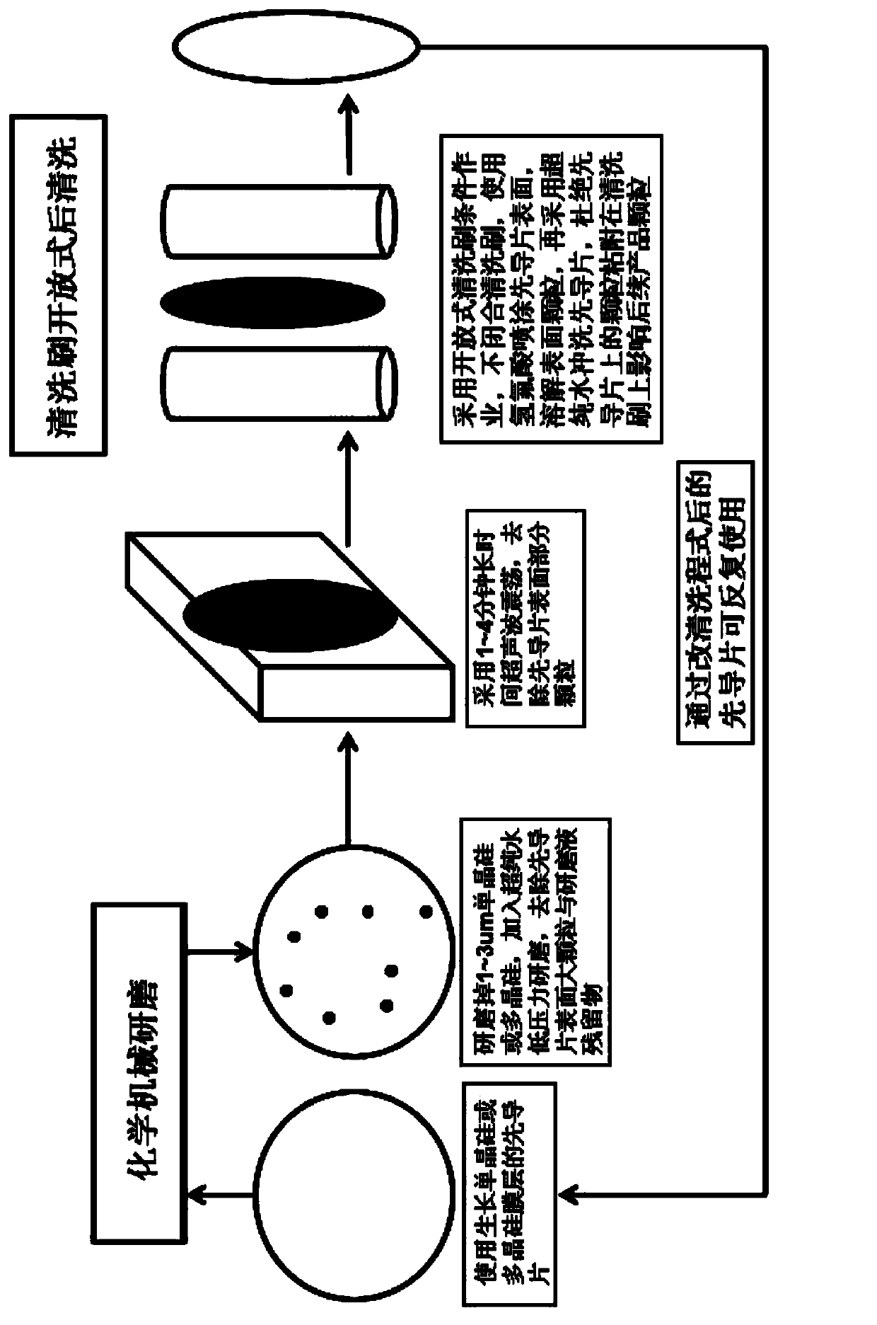
[0019] A kind of chemical mechanical grinding operation method of the present invention, its flow process is as follows image 3 As shown, the job method includes the following steps:

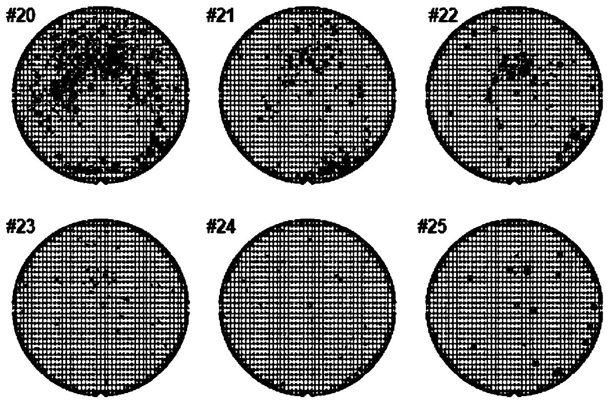
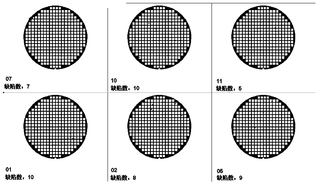
[0020] a: Use a silicon wafer growing a monocrystalline silicon or polycrystalline silicon film layer as a pilot wafer, the pilot wafer passes through a chemical mechanical grinding device, and after grinding the pilot wafer program, add a soft-haired grinding pad for grinding, use ultrapure water as the grinding liquid, and use 1 ~3PSI low pressure grinding for 1~3 minutes, grinding away about 1~3μm single crystal silicon or polycrystalline silicon, so as to remove large particles and grinding liquid residues on the surface of the pilot chip.

[0021] b: Ultrasonic cleaning is performed on the ground pilot plate, and the cleaning procedure adopts long-term ultrasonic vibration for 1 to 4 minutes to remove some particles on the surface of the pilot plate.

[0022] c: Use the cleaning program o...


PUM


Abstract

The invention discloses a chemical mechanical polishing operating method. The chemical mechanical polishing operating method includes that: using a monocrystalline silicon or polycrystalline silicon growth silicon wafer as a guide piece, wherein the guide piece is a dummy wafer which enables each performance index of a machine to arrive at a stable standard before operating; optimizing a polishing form, to be specific, optimizing to enable the surface of the repeatedly used guide piece to still have a diameter more than 0.20 micrometers and a particle number less than 50, cleaning the polishing guide piece in a cleaning brush opening mode, and closing the cleaning brush when operating the product so as to avoid the product particle increase due to the poor guide piece particle condition.

Description

technical field [0001] The invention relates to the field of semiconductor integrated circuit manufacturing, in particular to a chemical mechanical grinding operation method. Background technique [0002] Chemical Mechanical Polishing (CMP: Chemical Mechanical Polishing) is one of the key processes in semiconductor manufacturing. It is a removal process that achieves its purpose by combining chemical reactions and mechanical polishing. And we use it in the semi-conductive thin-film body process, and use it to peel off the film to make the surface smoother and more flat. It is also used in the metallization process of semiconductors to remove a large amount of metal film on the surface to form in-line plugs or metal lines in the dielectric film. And when the wafer is cut from the monocrystalline silicon ingot, many process steps are used to prepare a flat, bright and defect-free silicon wafer to meet the requirements of the integrated circuit process, and the chemical mechan...

Claims


Application Information

Patent Timeline
Patent Type & Authority Applications(China)
IPC IPC(8): B24B37/04
CPCB24B37/10H01L21/02013H01L21/3212
Inventor 唐锦来
Owner SHANGHAI HUAHONG GRACE SEMICON MFG CORP
Why Eureka
Try Eureka