Novel double-Y-waveguide integrated optical device and manufacturing method thereof

A waveguide integration and optical device technology, applied in optical components, optical waveguide light guides, optics, etc., can solve the problems of device volume reduction, low integration, multi-fiber fusion points, etc., to suppress the generation of parasitic waves and improve the device. performance, the effect of reducing parameter drift

Inactive Publication Date: 2014-06-18
THE 44TH INST OF CHINA ELECTRONICS TECH GROUP CORP
View PDF7 Cites 3 Cited by
  • Summary
  • Abstract
  • Description
  • Claims
  • Application Information

AI Technical Summary

Problems solved by technology

[0002] At present, the fiber optic gyroscope systems commonly used at home and abroad all use figure 1 The scheme shown includes a Y-waveguide chip, a light source, a detector, a coupler and an optical fiber ring. The problem is that the coupler and the Y-waveguide chip in the existing device are independent devices. The integration level is not high, the installation space takes up a lot, and the coupler and the Y waveguide chip need to be connected through a light-guiding optical fiber. There are many optical fiber fusion points inside the device, and the stability is poor.
[0003] For the foregoing problems, those skilled in the art have conducted a large amount of research and found a theoretically feasible solution, which is as follows: figure 2 As shown, the core of the scheme is to integrate the beam splitter / combiner and the polarizer / analyzer on the same chip (that is, by figure 2 The two bifurcated waveguide sections of the double Y-shaped waveguide are used as beam splitter / combiner and polarizer / analyzer respectively). In theory, this solution can effectively reduce the size of the device on the basis of greatly reducing the The number of light-guiding fibers inside the device and the number of corresponding fiber fusion points can effectively improve the reliability of the device from the structural aspect; but as mentioned above, this solution is only at the theoretical level. The reason is: from the light source The input light is first split at the first Y branch, after the first split, the optical power will be attenuated by half, the attenuated light continues to travel forward in the waveguide, and is split again at the second Y branch, and then transmitted According to the mode cut-off condition, a considerable part of the light will be radiated into the substrate and transmitted forward in the substrate according to the mode cut-off condition. According to the optical path transmission theory, this part of the radiated light will be in the A Y branch is coupled back into the waveguide, thereby causing spurious waves. The spurious waves are asymmetrical, and a spurious phase difference will be generated between the two transmission arms, resulting in the drift of the fiber optic gyroscope system parameters. When the temperature changes, This drift is particularly obvious, which seriously affects the practicability of the scheme, so this double Y-shaped waveguide has not been practically applied in engineering practice

Method used


Image

  • Novel double-Y-waveguide integrated optical device and manufacturing method thereof
  • Novel double-Y-waveguide integrated optical device and manufacturing method thereof
  • Novel double-Y-waveguide integrated optical device and manufacturing method thereof

Examples


Embodiment Construction

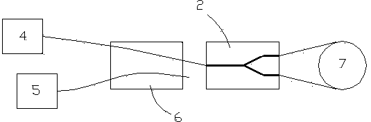
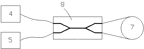
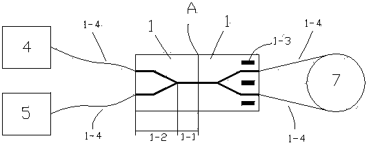
[0021] A novel double Y waveguide integrated optical device, the innovation of which is: the novel double Y waveguide integrated optical device is spliced ​​by two chips 1; the chip 1 is provided with a Y-shaped waveguide; the Y-shaped waveguide is composed of a direct The strip section 1-1 and the bifurcated section 1-2 are composed, and the end surface of the chip 1 that is flush with the outer end surface of the straight section 1-1 forms a connection end; the end surface of the connection end is coated with a light-absorbing material layer, and the light-absorbing material A bare area is provided in the middle of the area covered by the layer, and the outer end surface of the straight section 1-1 is located within the range of the exposed area; the connecting ends of the two chips 1 are spliced ​​together and fixed by a waveguide coupling process. After splicing, the two The straight segments 1-1 on the block chip 1 are coaxial.

[0022] Further, one of the two chips 1 is ...


PUM


Abstract

The invention provides a novel double-Y-waveguide integrated optical device and a manufacturing method of the novel double-Y-waveguide integrated optical device. The device is formed by splicing two chips. A Y type waveguide is arranged on each chip and is composed of a straight strip section and a fork section. The end, flush with the outer end face of the corresponding straight strip section, of each chip forms a connecting end. The end face of each connecting end is coated with a light absorption material layer. An exposed area is arranged in the middle of the area covered with each light absorption material layer. The outer end face of each straight strip section is located within the range of the corresponding exposed area. The connecting ends of the two chips are spliced together and fixed through the waveguide coupling process, and the straight strip sections of the two chips are coaxial after splicing is conducted. The novel double-Y-waveguide integrated optical device and the manufacturing method have the advantages that transmission of radiation light in the substrate can be effectively cut off, and therefore occurrence of extrancous waves is restrained, parameter drifting of an optical fiber gyro system is reduced, and the performance of the device is improved.

Description

technical field [0001] The invention relates to an optical device, in particular to a novel double Y waveguide integrated optical device and a manufacturing method thereof. Background technique [0002] At present, the fiber optic gyroscope systems commonly used at home and abroad all use figure 1 The scheme shown includes a Y-waveguide chip, a light source, a detector, a coupler and an optical fiber ring. The problem is that the coupler and the Y-waveguide chip in the existing device are independent devices. The integration level is not high, the installation space takes up a lot, and the coupler and the Y-waveguide chip need to be connected through a light-guiding optical fiber. There are many optical fiber fusion points inside the device, and the stability is poor. [0003] For the foregoing problems, those skilled in the art have conducted a large amount of research and found a theoretically feasible solution, which is as follows: figure 2 As shown, the core of th...

Claims


Application Information

Patent Timeline
Patent Type & Authority Applications(China)
IPC IPC(8): G02B6/125G02B6/13
Inventor 华勇张鸿举杨千泽刘隐郑德晟
Owner THE 44TH INST OF CHINA ELECTRONICS TECH GROUP CORP
Why Eureka
Try Eureka