A semiconductor power device layout

A power device and semiconductor technology, applied in the field of semiconductor power device layout, can solve problems such as excessive stress, increased chip thermal stress, and difficulty in continuing subsequent processes.

Active Publication Date: 2018-10-26
ZHUZHOU CRRC TIMES SEMICON CO LTD
View PDF6 Cites 1 Cited by
  • Summary
  • Abstract
  • Description
  • Claims
  • Application Information

AI Technical Summary

Problems solved by technology

[0007] As mentioned earlier, one aspect of chip stress comes from trench etching, deposition and other processes. figure 1 The gate trenches and virtual gate trenches of mid-power MOSFETs are all along a single horizontal direction, making the problem of excessive stress more serious. When the trenches are filled with oxide layers, polysilicon and other substances, the accumulation of stress may Can cause wafer warpage, making subsequent processes difficult to continue
on the other hand, Figure 2A The virtual gate contact hole of the medium power MOSFET is located at both ends of the virtual gate trench, and its width is greater than the width of the virtual gate trench. Since the virtual gate region is P-type, the hole carriers in the virtual gate region and the P+ gate contact region and the source A large amount of transmission between regions will not only affect the performance and reliability of the device, but also cause uneven distribution of local current on the chip and increase the thermal stress on the chip

Method used


Image

  • A semiconductor power device layout
  • A semiconductor power device layout
  • A semiconductor power device layout

Examples


Embodiment Construction

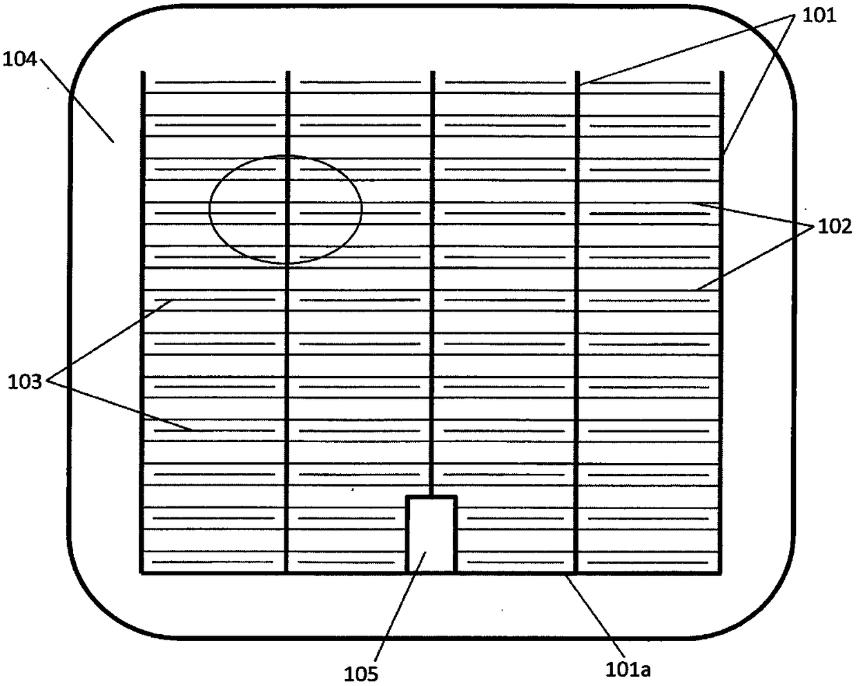
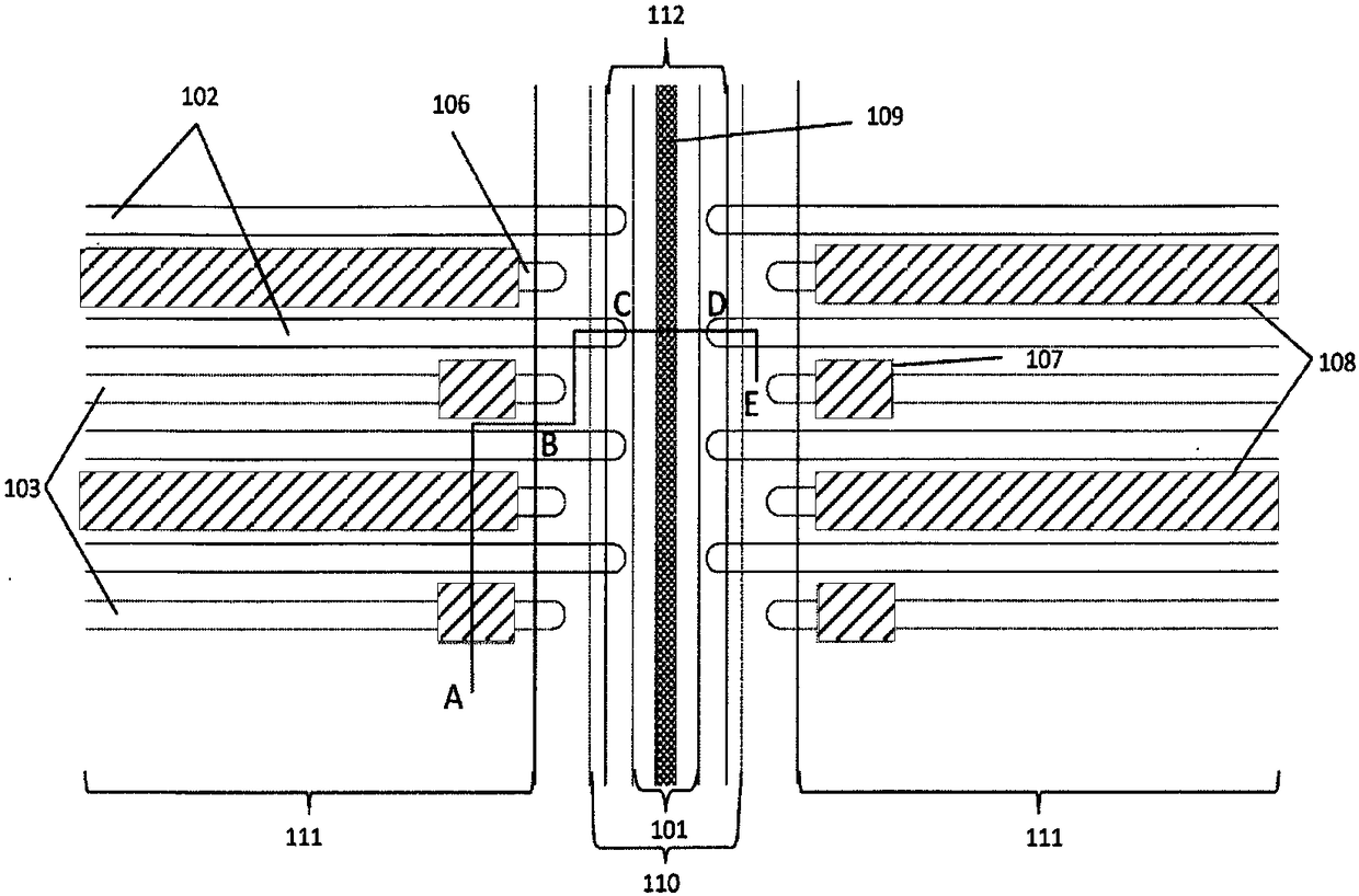
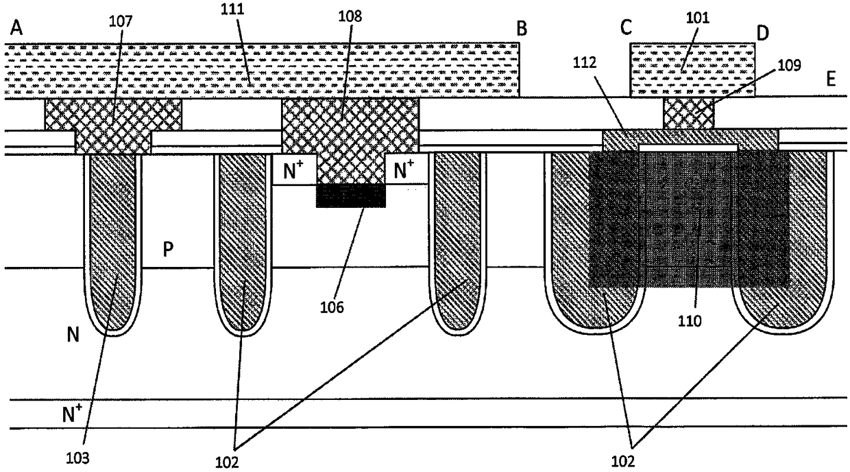
[0030] As mentioned in the background technology section, the gate trenches and dummy gate trenches of power MOSFETs in the prior art are all along a single horizontal direction, making the problem of excessive stress more serious. When the trenches are filled with an oxide layer , polysilicon and other substances, the accumulation of stress may cause the wafer to warp, making it difficult to continue the subsequent process. Width, because the dummy gate region is P-type, a large number of hole carriers are transported between the dummy gate region, the P+ gate contact region and the source region, which not only affects the performance and reliability of the device, but also causes uneven local current distribution on the chip. Both, increasing the thermal stress on the chip.

[0031]Based on this, an embodiment of the present invention provides a layout of a semiconductor power device, including a gate trench, a dummy gate trench, a base contact region, a dummy gate contact ...


PUM


Abstract

The invention discloses a semiconductor power device layout. The semiconductor power device layout is characterized in that the middle part of each grid groove is a broken line structure, two ends extend into grid contact areas and are connected with grid buses, and tail ends are mutually connected on the position with preset distances from the grid contact areas, and an enclosed virtual grating area is formed; virtual grating grooves are arranged in the enclosed virtual grating area and are parallel to the grid grooves, and enclosed contact windows are formed on two ends or the middle part of each virtual grating groove; a base region contact area is arranged between two adjacent grid grooves and is parallel to the grid grooves; virtual grating contact holes are formed in the enclosed contact windows on the virtual grating grooves, and the width of the virtual grating contact hole is larger than the width of the virtual grating groove; and a source electrode contact hole covers the base region contact area, the width of the source electrode contact hole is larger than the width of the base region contact area, and the length of the source electrode contact hole is smaller than length of the base region contact area. The grid grooves, the virtual grating grooves and the base region contact areas respectively comprises horizontal and non-horizontal parts, the grooves in different direction are capable of dispersing the stress on a chip, and the chip is enabled to be prepared by a thinner wafer.

Description

technical field [0001] The invention relates to the technical field of semiconductor device unit structure and layout, in particular to a semiconductor power device layout. Background technique [0002] For vertical semiconductor power devices, wafer thinning is an important way to increase power density. By reducing the thickness of the wafer, the on-resistance of the device can be reduced, thereby reducing power loss. Thinness can also reduce the thermal resistance of the chip and improve the heat dissipation capability of the chip. [0003] The advanced wafer thinning process can obtain wafers with very small thickness, but the ability of the chip to withstand various stresses is reduced after the thickness of the wafer is thinned. These stresses mainly come from two aspects. On the one hand, during the device preparation process, Processes such as trench etching and film deposition will cause different stress coefficients in different parts of the chip. This problem wil...

Claims


Application Information

Patent Timeline
Patent Type & Authority Patents(China)
IPC IPC(8): H01L27/02H01L29/78H01L29/06H01L29/423
CPCH01L27/0207H01L29/0684H01L29/4236H01L29/78
Inventor 郑昌伟戴小平
Owner ZHUZHOU CRRC TIMES SEMICON CO LTD
Why Eureka
Try Eureka