Optical sensor based on cascaded f-p semiconductor laser and thin-film f-p filter
A F-P and laser technology, applied in the field of optical sensors, can solve the problems of expensive, bulky, and difficult coupling of input and output light of optical waveguide sensors, and achieve the effect of increasing the working distance, improving sensitivity and increasing modulation
- Summary
- Abstract
- Description
- Claims
- Application Information
AI Technical Summary
Problems solved by technology
Method used
Image
Examples
Embodiment Construction
[0016] The present invention will be further described below in conjunction with the accompanying drawings and embodiments.
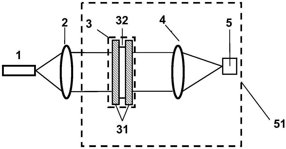
[0017] Such as figure 1 Shown, the present invention is a kind of optical sensor based on F-P semiconductor laser and thin-film F-P optical filter cascaded, comprises F-P semiconductor laser 1, collimating lens 2, thin-film F-P optical filter surface array 3, imaging lens 4 and detector surface array5. Wherein, the thin-film F-P filter surface array 3, the imaging lens 4 and the detector surface array 5 form a filter surface array 51 of a periodic filter spectrum; The spacer layer between the film layers 31 serves as the sensing area 32 .
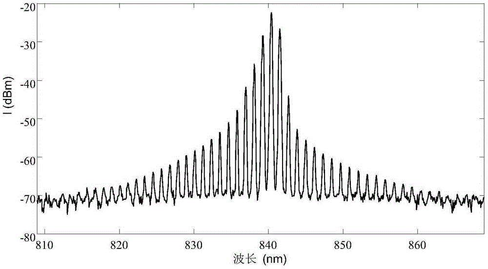
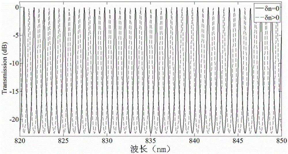
[0018] The light source of the F-P semiconductor laser 1 becomes parallel light after passing through the collimating lens 2, and is vertically incident on the thin film F-P filter surface array 3, and the transmitted light passes through the imaging lens 4, and is imaged on the detector surface array 5, and the de...
PUM
 Abstract
Description
Claims
Application Information


