Method for measuring size of nonbonding area on bonding device structure

A device structure and bonding technology, which is applied in the direction of semiconductor/solid-state device testing/measurement, electrical components, circuits, etc., can solve the problems of structural damage and poor measurement accuracy of the bonded device to be tested, and achieve strong practicability and economical Low production cost and wide range of applications

Inactive Publication Date: 2014-06-25
WUHAN XINXIN SEMICON MFG CO LTD
View PDF5 Cites 1 Cited by
  • Summary
  • Abstract
  • Description
  • Claims
  • Application Information

AI Technical Summary

Problems solved by technology

[0007] In view of the above problems, the present invention provides a method for obtaining the size of the non-bonded region of the bonded device structure to be tested by irradiating the Newton rings generated by the bonded device structure to be tested by a light source that can penetrate the bonded device structure to be tested, which solves the problem of In the prior art, the measurement accuracy of the size of the non-bonded area on the structure of the bonded device to be tested is poor, and the problem that the structure of the bonded device to be tested will be damaged while detecting the size of the non-bonded area of ​​the wafer

Method used


Image

  • Method for measuring size of nonbonding area on bonding device structure
  • Method for measuring size of nonbonding area on bonding device structure
  • Method for measuring size of nonbonding area on bonding device structure

Examples


Embodiment Construction

[0029] The present invention will be further described below in conjunction with the accompanying drawings and specific embodiments, but not as a limitation of the present invention.

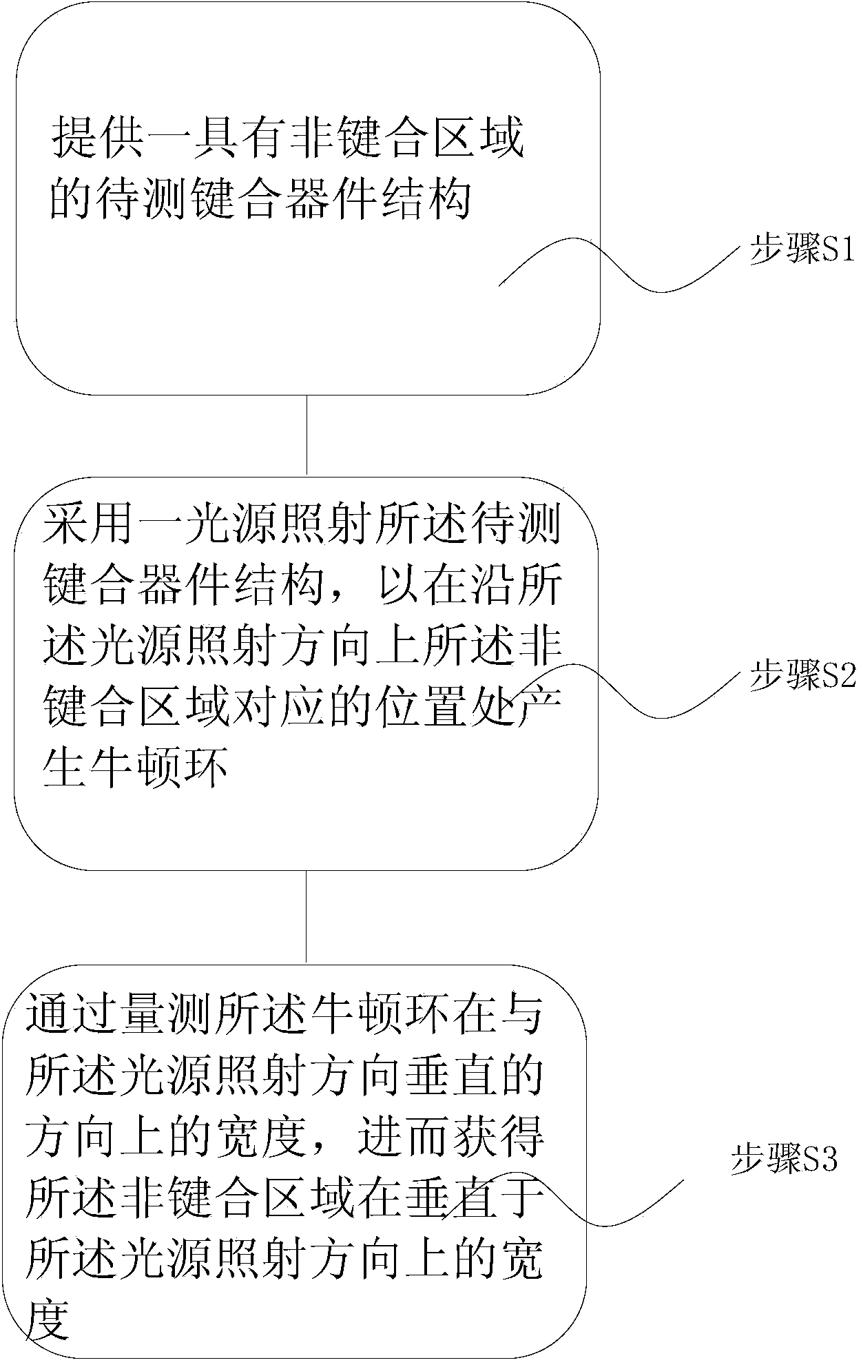
[0030] figure 1 It is a schematic flow chart of the method for measuring the size of the non-bonded area on the structure of the bonded device in the embodiment of the present invention, such as figure 1 Shown:

[0031] This embodiment relates to a method for measuring the size of a non-bonded area on a bonded device structure, the method comprising the following steps:

[0032] Step S1, providing a bonding device structure to be tested with at least one non-bonding region.

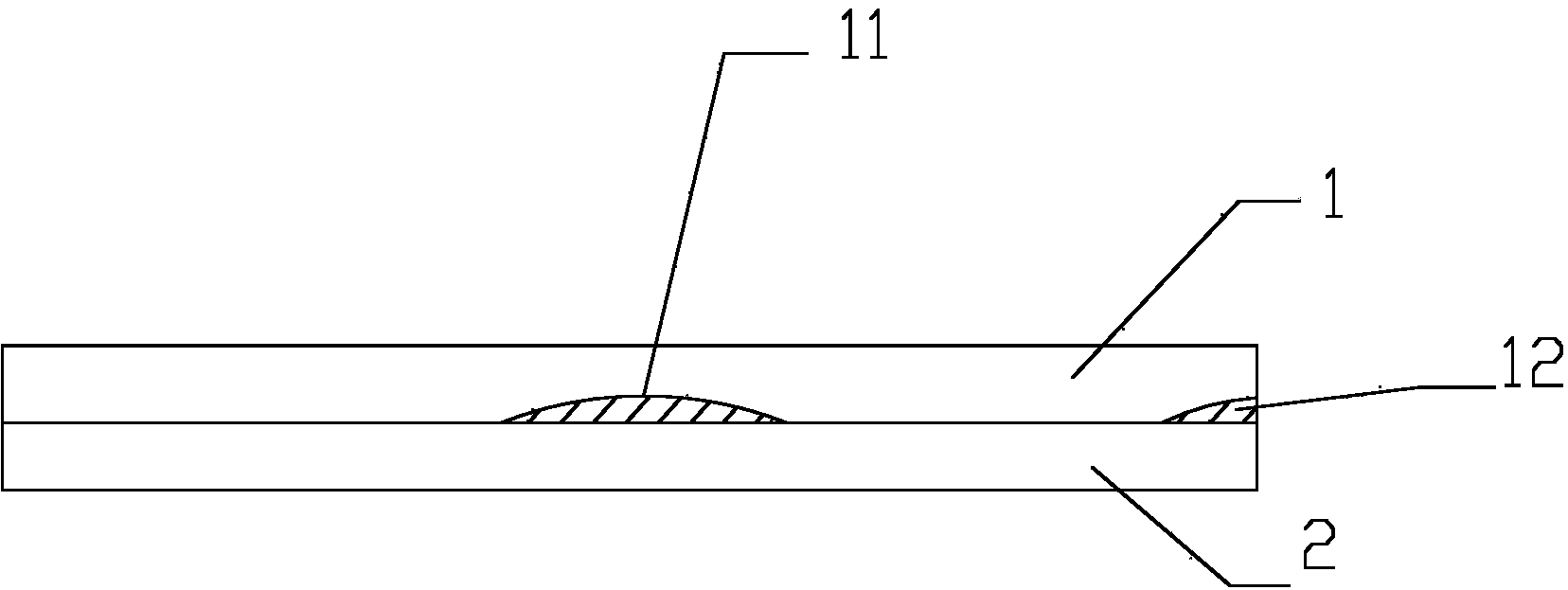
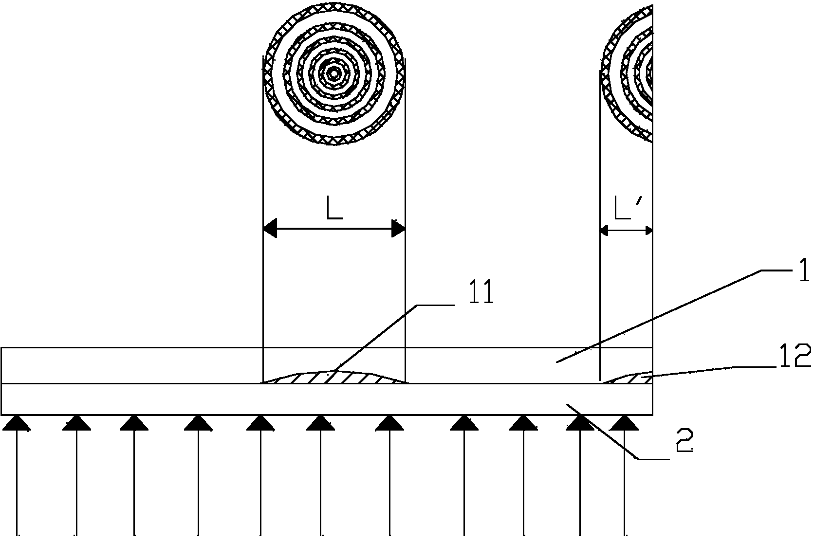
[0033] figure 2 It is a schematic cross-sectional view of a bonded device structure to be tested with a non-bonding region in an embodiment of the method of the present invention; as figure 2 As shown, the substrate of the bonded device structure to be tested is a wafer, namely figure 2 It is a bonded wafer formed b...


PUM


Abstract

The invention discloses a method for measuring the size of a nonbonding area on a bonding device structure. According to the method, light capable of penetrating through the bonding device structure to be measured is adopted to shine on the bonding device structure to be measured so that a Newton ring can be formed at the position corresponding to the nonbonding area in the light incidence direction, then the width, in the direction perpendicular to the light incidence direction, of the Newton ring is measured by means of an optical measuring microscope, and then the width, in the direction perpendicular to the light incidence direction, of the nonbonding area is obtained. According to the method, the measurement of the size of the nonbonding area on the bonding device structure is achieved by means of the Newton ring principle, an accurate measurement result can be obtained, no damage can be caused to the bonding device structure to be measured serving as a sample during measurement, and then production cost is reduced. Furthermore, the method can be applied to bonding device structures formed by bonding of wafers the thickness of each of which is o micron - 775 microns, or chips or other silicon substrates, the method supports substrate doping, the application range is wide, and practicality is high.

Description

technical field [0001] The invention relates to the technical field of semiconductor manufacturing, in particular to a method for measuring the size of a non-bonded area on a bonded device structure. Background technique [0002] At present, the wafer bonding technology is widely used in semiconductor integrated manufacturing, so the detection of the size of the non-bonding area in the wafer bonding technology is particularly important, and thus becomes an important topic. The current commonly used method is to use the acoustic characteristics of the ultrasonic microscope (SAM) to detect the size of the non-bonding area in the bonded wafer, and use the acoustic properties of the ultrasonic microscope (SAM) to detect the size of the non-bonding area, and its accuracy Low, and for the detection of the non-bonding area on the edge of the sample, the water medium used will affect the measurement of the gap spacing, and cannot reflect the size of the non-bonding area most truly, ...

Claims


Application Information

Patent Timeline
Patent Type & Authority Applications(China)
IPC IPC(8): H01L21/66
CPCH01L22/12
Inventor 胡思平陈俊朱继锋
Owner WUHAN XINXIN SEMICON MFG CO LTD
Why Eureka
Try Eureka