Method for using scanning machine program to detect wafers according to floating threshold values

A scanning machine, floating threshold technology, used in semiconductor/solid-state device testing/measurement, electrical components, circuits, etc., can solve the problem of reducing the number of false alarms that exceed specifications, and achieve the effect of reducing the number and eliminating the impact of noise defects

Inactive Publication Date: 2014-06-25
SHANGHAI HUALI MICROELECTRONICS CORP
View PDF4 Cites 5 Cited by
  • Summary
  • Abstract
  • Description
  • Claims
  • Application Information

AI Technical Summary

Problems solved by technology

[0003] In order to overcome the deficiencies in the above-mentioned prior art, the object of the present invention is to provide a method for wafer detection by a scanning machine program using a floating threshold, which collects relevant data of the front layer in the wafer manufacturing process through the scanning machine, and then One or more thresholds are calculated by the machine fitting function, and the floating threshold is used for defect scanning to eliminate the influence of noise defects caused by small process differences between wafers, thereby reducing the number of false alarms that exceed specifications

Method used


Image

  • Method for using scanning machine program to detect wafers according to floating threshold values
  • Method for using scanning machine program to detect wafers according to floating threshold values
  • Method for using scanning machine program to detect wafers according to floating threshold values

Examples


Embodiment Construction

[0020] The implementation of the present invention is described below through specific examples and in conjunction with the accompanying drawings, and those skilled in the art can easily understand other advantages and effects of the present invention from the content disclosed in this specification. The present invention can also be implemented or applied through other different specific examples, and various modifications and changes can be made to the details in this specification based on different viewpoints and applications without departing from the spirit of the present invention.

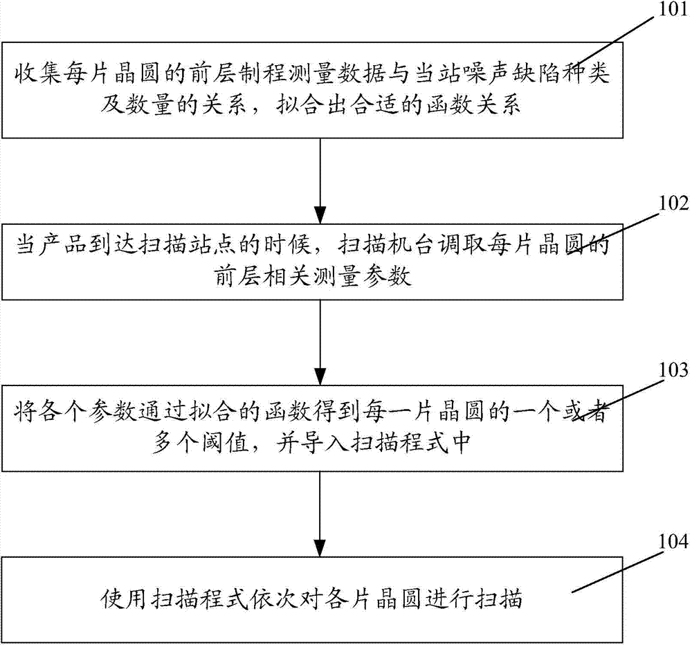
[0021] figure 1 It is a flow chart of the steps of the method for wafer detection by the scanning machine program of the present invention using floating thresholds. Such as figure 1 As shown, a scanning machine program of the present invention uses a floating threshold for wafer detection, comprising the following steps:

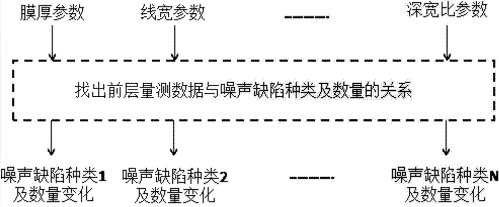
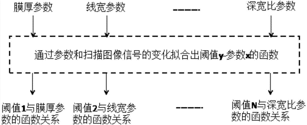
[0022] Step 101, collect the relationship between the front-layer...


PUM


Abstract

The invention discloses a method for using a scanning machine program to detect wafers according to floating threshold values. The method includes the first step of collecting the relations between front-layer processing measurement data of each wafer and the type of noise defects at a current site and the relations between the front-layer processing measurement data of each wafer and the number of the noise defects at the current site and fitting the function relationship between the threshold values and parameters, the second step of allowing a scanning machine to call front-layer processing measurement parameters of each wafer when a product reaches a scanning site, and the third step of substituting the parameters into a fitting function in the first step to obtain one or more threshold values of each wafer, leading the threshold values into the scanning program and scanning each wafer according to the threshold values of each wafer by using the scanning program sequentially. According to the method, the related front-layer processing data of the wafers in the manufacturing process are collected through the scanning machine, then one or more threshold values are obtained through the fitting function calculation of the scanning machine, defect scanning is carried out according to the floating threshold values so as to eliminate influences of noise defects caused by tiny processing difference between the wafers, and consequently the number of the wafers with specifications exceeding false-alarm can be reduced.

Description

technical field [0001] The invention relates to the fields of microelectronics manufacturing and semiconductor testing, in particular to a method for wafer detection by a scanning machine program using a floating threshold. Background technique [0002] Today's semiconductor industry's online wafer inspection mainly relies on various scanning machines, and its scanning mechanism is mainly based on light / electron incident on the wafer surface, collecting reflected / scattered light / electrons, and obtaining a grayscale image. The perfect unit is compared with it to obtain the gray difference value, and then according to one or more fixed thresholds set before, it is considered a defect if one or more thresholds are exceeded. However, there are always slight differences in the manufacturing process, resulting in differences in film thickness, warpage, line width, aspect ratio and other parameters between wafers. Changes in these factors will change the noise defects of the scanni...

Claims


Application Information

Patent Timeline
Patent Type & Authority Applications(China)
IPC IPC(8): H01L21/66
CPCH01L22/12H01L22/26
Inventor 郭贤权许向辉何理陈超
Owner SHANGHAI HUALI MICROELECTRONICS CORP
Why Eureka
Try Eureka