Image sensing device and method of operation thereof

An image sensing device and pixel unit technology, applied in the field of image sensing, can solve the problems of uneven exposure time of pixel units, large shot noise, affecting the authenticity of images, etc., so as to overcome the uneven exposure time and reduce shot Noise, the effect of simplifying the overall area

Active Publication Date: 2017-03-22
SHANGHAI ADVANCED RES INST CHINESE ACADEMY OF SCI
View PDF3 Cites 0 Cited by
  • Summary
  • Abstract
  • Description
  • Claims
  • Application Information

AI Technical Summary

Problems solved by technology

[0005] In view of the shortcomings of the prior art described above, the purpose of the present invention is to provide an image sensing device and its operating method, which are used to solve the problem of uneven exposure time of pixel units in the prior art, large shot noise during image sensing, and thus affecting the authenticity of the image

Method used


Image

  • Image sensing device and method of operation thereof
  • Image sensing device and method of operation thereof
  • Image sensing device and method of operation thereof

Examples


Embodiment Construction

[0059] Embodiments of the present invention are described below through specific examples, and those skilled in the art can easily understand other advantages and effects of the present invention from the content disclosed in this specification. The present invention can also be implemented or applied through other different specific implementation modes, and various modifications or changes can be made to the details in this specification based on different viewpoints and applications without departing from the spirit of the present invention.

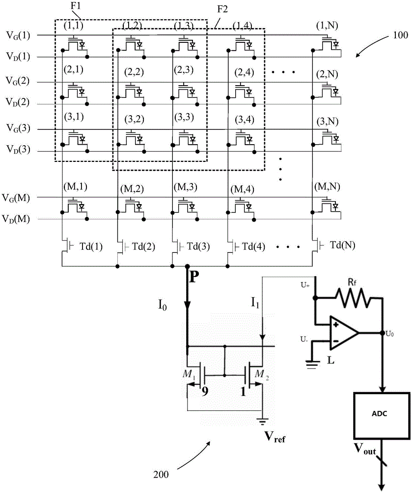
[0060] see figure 1 Schematic diagram of the image sensing device of the present invention.

[0061] It should be noted that the diagrams provided in this embodiment are only schematically illustrating the basic idea of ​​the present invention, and only the components related to the present invention are shown in the diagrams rather than the number, shape and shape of the components in actual implementation. Dimensional drawing, the ...


PUM


Abstract

The invention provides an image sensing device and an operation method thereof. The image sensing device at least comprises a pixel array and a read-out circuit, wherein the pixel array comprises a plurality of sub arrays, each sub array comprises i*j pixel units, i is the number of rows, j is the number of columns, i is larger than or equal to two, j is larger than or equal to two, control grids of the pixel units in the same row are connected with the same work line, drain electrodes of the pixel units in the same row are connected with the same control line, source electrodes of the pixel units in the same column are connected with bit lines, the pixel units in the sub arrays become light-sensitive under the action of voltage of predetermined word lines and control lines and generate output currents of the i*j pixel units, the output currents are output to the read-out circuit through the bit lines, and the read-out circuit is used for collecting and averaging the output currents and converting the averaged currents into voltage to be output to an external circuit. The image sensing device and the operation method solve the problem that exposure time of the pixel units is not uniform, lower shot noise of an image and improve the visual effect of the image.

Description

technical field [0001] The invention relates to image sensing technology, in particular to an image sensing device and an operating method thereof. Background technique [0002] As we all know, an image sensor is a semiconductor device that converts an optical image into an electrical signal. Image sensors can be roughly classified into charge-coupled device (Charge-Coupled Device, CCD for short) and complementary metal oxide semiconductor (Complementary Metal Oxide Semiconductor, CMOS for short) image sensors. [0003] Whether it is a CCD or a CMOS image sensor, the photosensitive signal is read out by scanning each pixel one by one. When light is irradiated on a pixel unit, a photosensitive device such as a photodiode is charged to a corresponding The level of the amount of light on a pixel. Once a charge is stored on the photosensitive device, the charge can be used to generate electrical pulses representing corresponding light levels. This electrical pulse is usually ...

Claims


Application Information

Patent Timeline
Patent Type & Authority Patents(China)
IPC IPC(8): H04N5/374H04N5/378H01L27/146
Inventor 汪辉黄成强章琦汪宁田犁方娜封松林
Owner SHANGHAI ADVANCED RES INST CHINESE ACADEMY OF SCI
Why Eureka
Try Eureka