Wafer level vacuum encapsulation of microelectron mechanical system and upside-down mounting soldering method thereof

A micro-electronic machinery and vacuum packaging technology, applied in opto-mechanical equipment, microstructure devices, chemical instruments and methods, etc., can solve the problems of rare reports on the application of MEMS devices, and achieve the improvement of overall performance and yield, high packaging density, The effect of improving accuracy and yield

Inactive Publication Date: 2009-07-15
PEKING UNIV
View PDF6 Cites 0 Cited by
  • Summary
  • Abstract
  • Description
  • Claims
  • Application Information

AI Technical Summary

Problems solved by technology

In addition, flip-chip technology has been widely used in integrated circuits, but its application in MEMS devices is rarely reported.

Method used


Image

  • Wafer level vacuum encapsulation of microelectron mechanical system and upside-down mounting soldering method thereof
  • Wafer level vacuum encapsulation of microelectron mechanical system and upside-down mounting soldering method thereof
  • Wafer level vacuum encapsulation of microelectron mechanical system and upside-down mounting soldering method thereof

Examples


Embodiment Construction

[0021] The present invention will be described in detail below in conjunction with the accompanying drawings and embodiments.

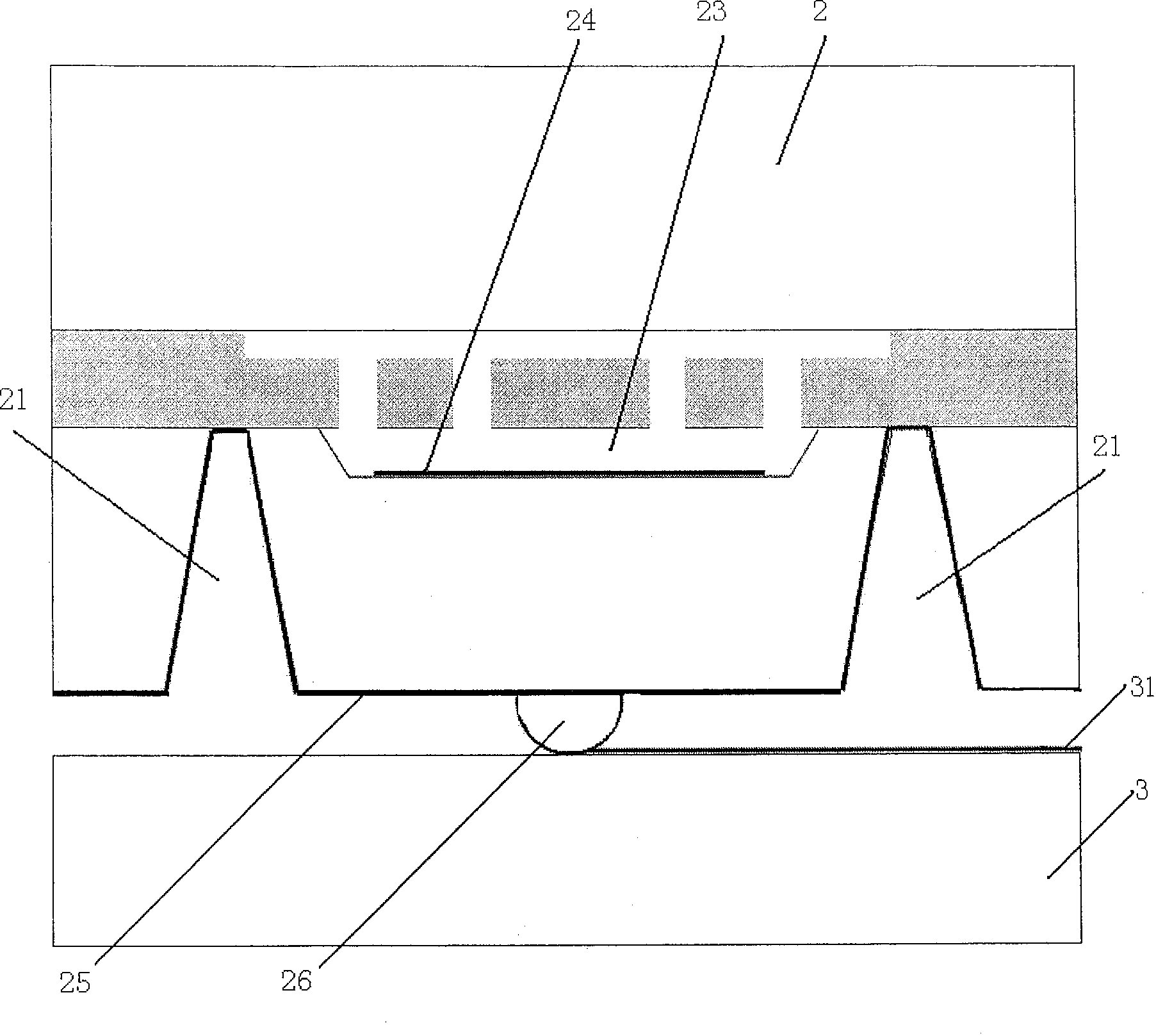
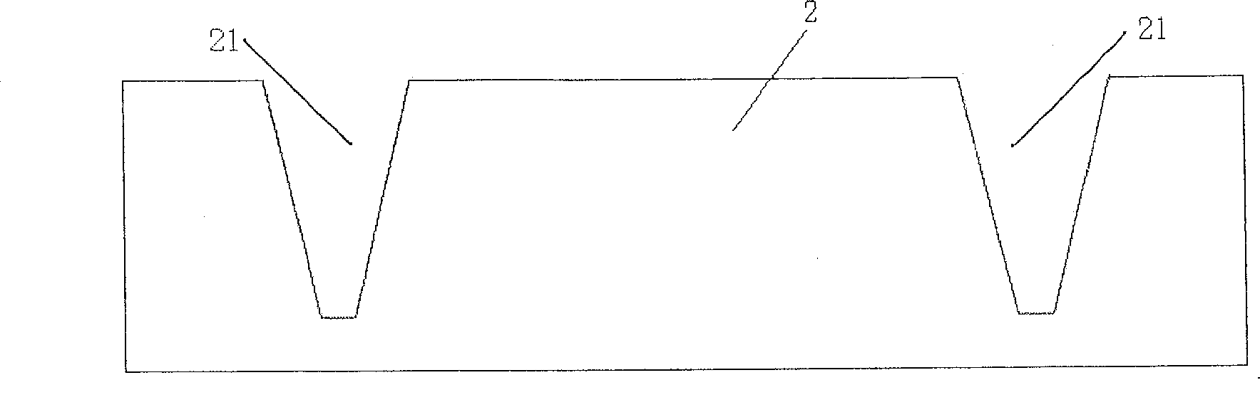
[0022] Such as figure 1 As shown, the present invention is mainly composed of a MEMS device structure wafer 1 , a cap glass wafer 2 and a peripheral processing circuit 3 . A MEMS device structure wafer 1 is composed of several hundred (determined by the size of the MEMS device chip) independent MEMS device chips. There are hundreds of vertical lead holes 21 on the cap glass sheet 2, and the number of lead holes 21 is equal to the product of the number of MEMS device chips on the MEMS device structure wafer 1 and the number of electrodes of the MEMS device chips. 2, process hundreds of glass cavities 23 (the number of the glass cavities corresponds to the number of MEMS chips), to protect the structure of the MEMS device chip, the glass cavities 23 are sputtered or coated with a getter 24 , the electrode leads 25 are placed in the lead holes 21, and ...


PUM

PropertyMeasurementUnit
thicknessaaaaaaaaaa
thicknessaaaaaaaaaa
thicknessaaaaaaaaaa

Abstract

The invention relates to the wafer level vacuum package and the flip chip method of the microelectromechanical system, which comprises the following steps: nut cap glass sheets are perforated without getting through; tungsten alloy or chrome alloy is spattered on one side without perforating pin holes on the nut cap glass sheets and photoetching and corrosion are performed to form masks; the hydrofluoric acid is used to erode the glass cavity and erode through the pin holes without puncturing through; getter is spattered in the glass cavity; MEMS static electricity device structure wafers and the nut cap glass sheets are bonded by static electricity under the high temperature and the low pressure; metal electrodes are fabricated on the nut cap glass sheets and metal bumps are fabricated on the metal electrodes; single MEMS device chip after cutting is packaged with processing circuits by flip chip. The method package of the invention can be used in batch production, protect the MEMS device chips from outer pollution and damage and increase the pass-rate of production. The invention can be widely applied in the MEMS system.

Description

technical field [0001] The invention relates to a micro-electro-mechanical system, in particular to a wafer-level vacuum packaging and flip-chip welding method of the micro-electro-mechanical system. Background technique [0002] The packaging technology of microelectromechanical systems (MEMS) is an important content of MEMS research at present. The feature size of MEMS devices is small, generally on the order of microns, and is easily affected by external environmental noise, or contaminated by moisture and dust in the air, resulting in degradation of device performance, and even failure in severe cases. Therefore, airtightness is required in most cases Or vacuum packaging to ensure the normal operation of the device. For some MEMS sensors, such as resonators and micro gyroscopes, vacuum packaging can significantly improve the quality factor Q value and sensitivity of the device, reduce the impact of environmental noise, and greatly improve the overall performance of the ...

Claims


Application Information

Patent Timeline
Patent Type & Authority Patents(China)
IPC IPC(8): B81C3/00B81C5/00B81C99/00
Inventor 丁海涛杨振川郭中洋迟晓珠赵前程郝一龙闫桂珍
Owner PEKING UNIV
Why Eureka
Try Eureka