Methods and structures for electrostatic discharge protection

a technology of electrostatic discharge and structure, applied in the direction of emergency protective arrangements for limiting excess voltage/current, pulse technique, etc., can solve the problems of many limitations, severe damage to the susceptible to damage to the semiconductor devices in the integrated circuit, etc., to improve esd protection and improve esd protection structure

Active Publication Date: 2010-05-06
MACRONIX INT CO LTD
View PDF6 Cites 21 Cited by
  • Summary
  • Abstract
  • Description
  • Claims
  • Application Information

AI Technical Summary

Benefits of technology

[0012]Many benefits are achieved by way of the present invention over conventional techniques. For example, in an embodiment, the invention provides ESD protection structures having lower trigger voltages for improved ESD protection. In specific embodiments, the improved ESD protection structures include a switch device coupled to an ESD current path. In various embodiments, the invention provides improved ESD protection structures for various devices, such as LDMOS, high voltage field transistor, and low voltage MOSFET. Depending upon the embodiment, one or more of these benefits may be achieved. These and other benefits will be described in more detail throughout the present specification and more particularly below.
[0013]Various additional objects, features and advantages of the present invention can be more fully appreciated with reference to the detailed description and accompanying drawings that follow.

Problems solved by technology

Semiconductor devices in an integrated circuit are susceptible to damages caused by electro-static discharge (ESD).
The high energy pulses of the electro-static discharge (ESD) can cause severe damage to the devices in the integrated circuits.
Even though conventional ESD protection structures are useful in some applications, many limitations still exist.
For example, conventional ESD protection structures often have high trigger voltages.
In certain applications, such high trigger voltages do not provide adequate ESD protection to the integrated circuit.

Method used


Image

  • Methods and structures for electrostatic discharge protection
  • Methods and structures for electrostatic discharge protection
  • Methods and structures for electrostatic discharge protection

Examples


Embodiment Construction

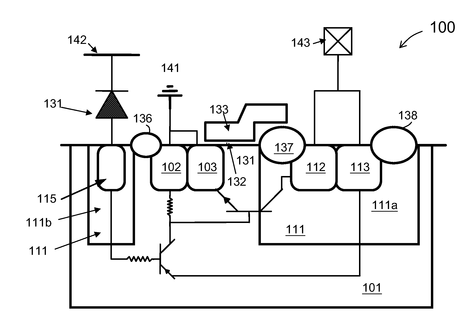
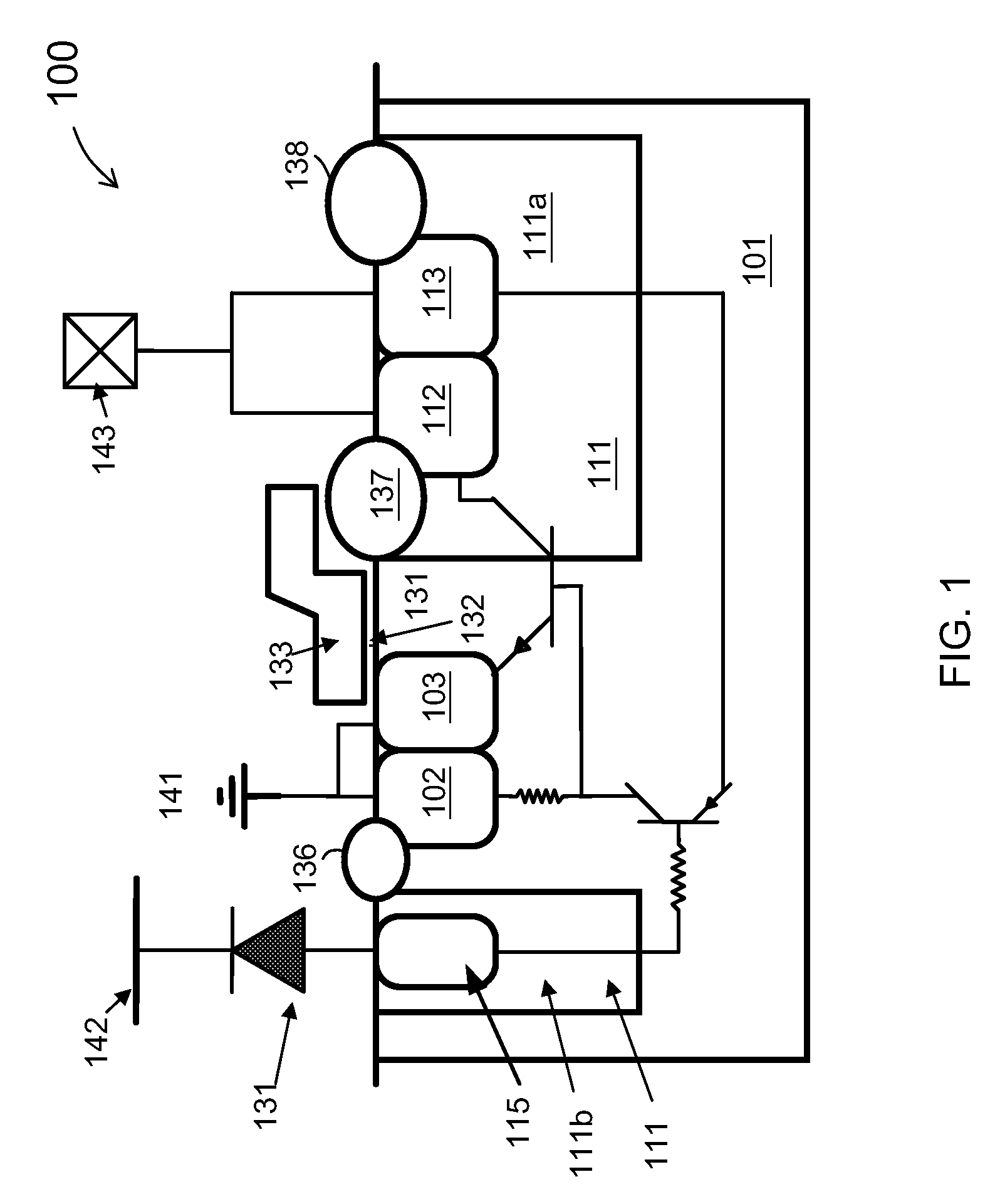
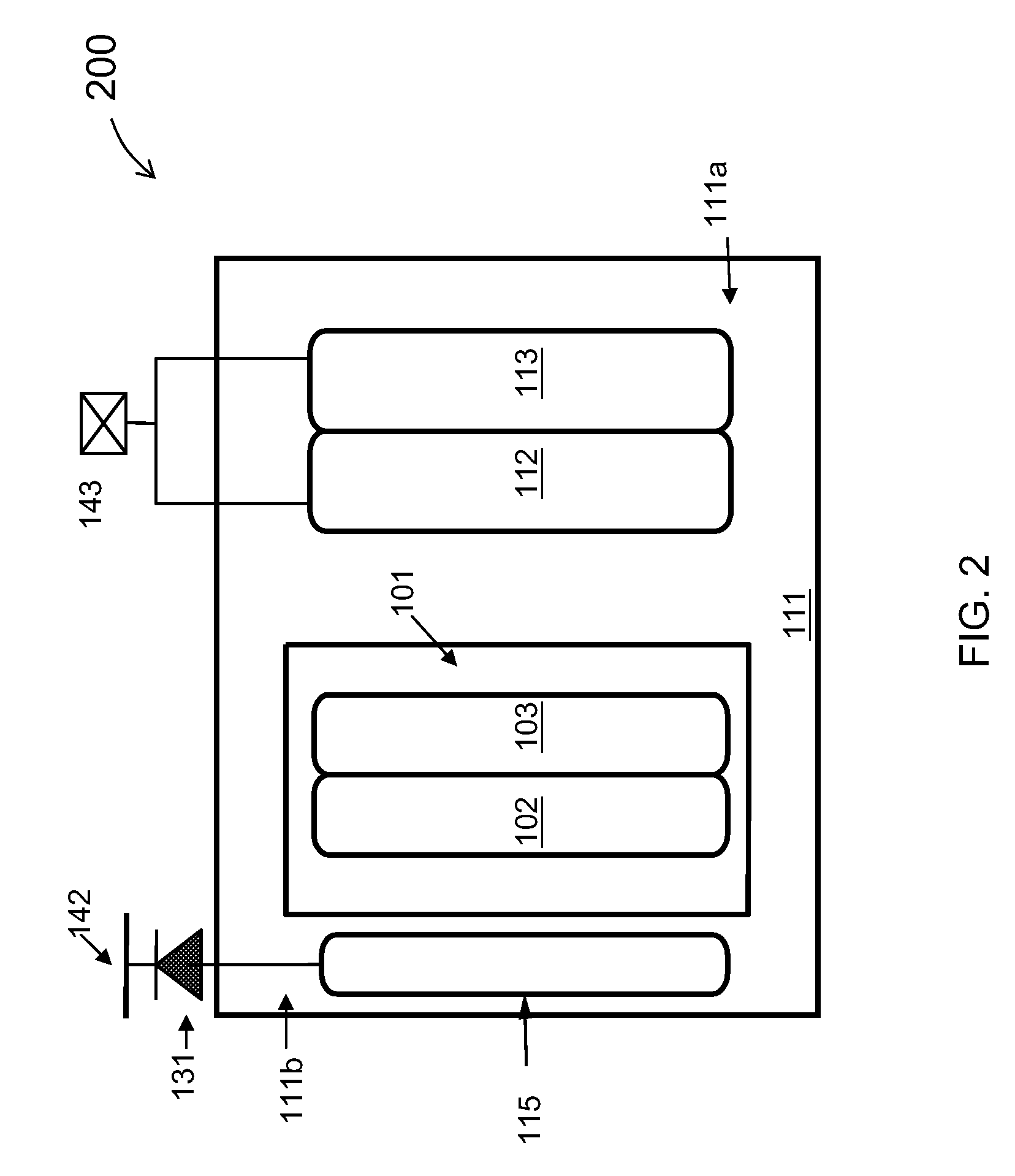
[0034]The present invention is directed to integrated circuits. More particularly, the invention provides a device for integrated circuits having electrostatic discharge (ESD) protection structure for providing an ESD current path which has a lower trigger voltage than a convention npn bipolar and silicon controlled rectifier (SCR). Merely by way of example, the invention has been applied to LDMOS lateral double-diffused MOSFET (LDMOS), high voltage field transistors, and low voltage MOSFET for improved ESD protection. But it would be recognized that the invention has a much broader range of applicability.

[0035]As discussed above, conventional ESD protection device structures based on SCR often have high trigger voltages. In a conventional ESD protection structure, the SCR and npn are often turned on, or triggered, if a high voltage at the drain contact pad is high enough to cause an avalanche breakdown at the junction between the n-well and p-substrate. This tends to result in a hi...


PUM


Abstract

A semiconductor device includes a first well region of a first conductivity, a second well region of a second conductivity type, a source region of the second conductivity type within the first well region, and a drain region of the second conductivity type at least partially within the second well region. A well contact to the first well region is coupled to the source. A third doped region of the first conductivity type and a fourth doped region of the second conductivity type are located in the second well region. A first transistor includes the third doped region, the second well region, and the first well region. The first transistor is coupled to a switch device. A second transistor includes the second well region, the first well region, and the source region. The first and the second transistors are configured to provide a current path during an ESD event.

Description

CROSS-REFERENCE TO RELATED APPLICATIONS[0001]This application is a continuation-in-part of U.S. patent application Ser. No. 12 / 264,879, filed Nov. 4, 2008, commonly assigned, which is incorporated in their entirety by reference for all purposes.BACKGROUND OF THE INVENTION[0002]Semiconductor devices in an integrated circuit are susceptible to damages caused by electro-static discharge (ESD). ESD can be induced by the motion of static electricity generated from a non-conductive surface. For example, a human body moving on a carpet may gather thousands of volts of static electricity. Moreover, in integrated circuits testing or packaging environment, even higher static electricity may be generated. The high energy pulses of the electro-static discharge (ESD) can cause severe damage to the devices in the integrated circuits.[0003]To prevent the damage of the integrated circuits due to the electro-static discharge, an ESD protection circuit is often included in the integrated circuit. Con...

Claims


Application Information

Patent Timeline
Patent Type & Authority Applications(United States)
IPC IPC(8): H01L29/73
CPCH01L27/0251H01L27/0262H01L29/0692H01L29/7436H01L29/78H01L29/7835H03K17/08H03K19/003H01L2924/0002H01L2924/00
Inventor WANG, SHIH-YULU, CHIA-LINGCHEN, YAN-YULIU, YU-LIENLU, TAO-CHENG
Owner MACRONIX INT CO LTD
Why Eureka
Try Eureka