
Interdigitated back-contact photovoltaic cells with floating front-emitter regions

A technology for photovoltaic cells and emitter regions, which is applied in photovoltaic power generation, circuits, electrical components, etc., and can solve problems such as complex manufacturing processes

Inactive Publication Date: 2016-02-10
STICHTING ENERGIEONDERZOEK CENT NEDERLAND
View PDF4 Cites 0 Cited by
  • Summary
  • Abstract
  • Description
  • Claims
  • Application Information

AI Technical Summary

Problems solved by technology

However, reducing the feature width makes the manufacturing process more complex

Method used


Image

  • Interdigitated back-contact photovoltaic cells with floating front-emitter regions
  • Interdigitated back-contact photovoltaic cells with floating front-emitter regions
  • Interdigitated back-contact photovoltaic cells with floating front-emitter regions

Examples


Embodiment Construction

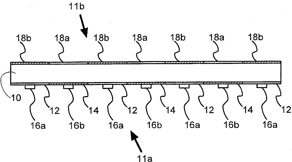
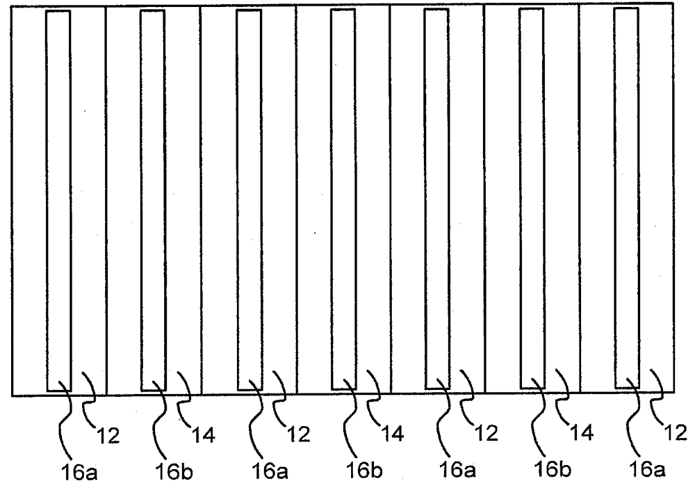
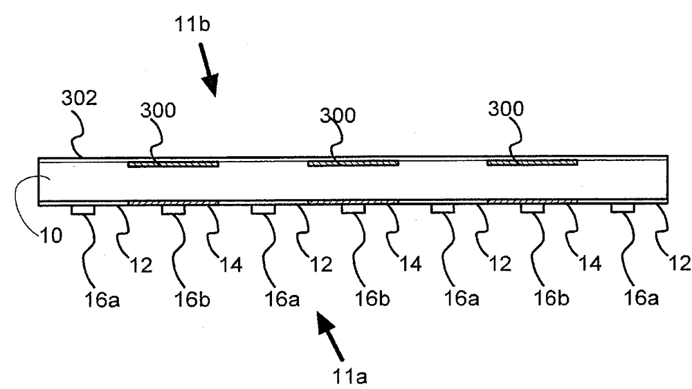
[0019] figure 1 Shown is a schematic cross-section of a photovoltaic cell comprising a semiconductor substrate 10 having a first surface and a second surface 11a, 11b, a base region 12 and an emitter region 14 on the first surface 11a , the first wire and the second wire 16a, 16b on the base region 12 and the emitter region 14 respectively, and other regions 18a, b of opposite conductivity types on the second surface 11b.

[0020] The semiconductor substrate 10 may be made of silicon, for example, silicon doped to have a first conductivity type (n-type or p-type) and have a thickness D in the range of 0.01-1000 microns, and more preferably 1-200 microns, This forms the distance between the first surface 11a and the second surface 11b. The first surface 11a and the second surface 11b of the semiconductor substrate 10 will be referred to as the back and the front, respectively, since the latter will face the sun or other source of light during operation, while the former will f...


PUM

PropertyMeasurementUnit
Widthaaaaaaaaaa

Abstract

A photovoltaic cell having a semiconductor substrate of a first conductivity type, the back surface of the semiconductor substrate having a base surface region and an emitter surface region of a first pattern, the base surface region and the emitter surface region being respectively coupled to a second One and the second output terminal. The first further surface area having the second pattern and the second further surface area on the front side are electrically floating with respect to the first and second output terminals. The first further surface region and the second further surface region have a first conductivity type and a second conductivity type, respectively. The first further surface region and the second further surface region at least partially overlap the emitter region and the base region, respectively, when viewed in projection in a direction perpendicular to the first surface.

Description

technical field [0001] The invention relates to a photovoltaic cell and a method of manufacturing the same. Background technique [0002] An interdigitated back contact photovoltaic cell has base and emitter regions on the same surface (commonly referred to as the back) of the photovoltaic cell. As is known per se, the operation of a photovoltaic cell is based on the light-induced excitation of free charge carriers in a semiconductor substrate. The base region and the emitter region are regions of opposite conductivity types that collect the majority and minority charge carriers, respectively, from the semiconductor substrate. [0003] Two different basic photovoltaic cell designs can be distinguished: those in which the base and emitter regions are arranged on opposite surfaces of a semiconductor substrate, and those in which the base and emitter regions are arranged on the same surface (back) of the substrate. type design. In interdigitated designs, the contacts of the ...

Claims


Application Information

Patent Timeline
IPC IPC(8): H01L31/0224H01L31/0352
CPCH01L31/022441H01L31/0682Y02E10/547H01L31/02008H01L31/022458H01L31/0236
Inventor 伊尔卡伊·赛萨尔
Owner STICHTING ENERGIEONDERZOEK CENT NEDERLAND
Learn More