Array substrate, manufacturing method of array substrate and display device

An array substrate and display area technology, which is applied in semiconductor/solid-state device manufacturing, semiconductor/solid-state device components, instruments, etc., can solve the problems of waste of company interests, irreparability, and bad influence on the company's quality image, so as to improve the utilization rate Low, reduced risk of injury effect

Inactive Publication Date: 2014-07-02
BOE TECH GRP CO LTD +1
View PDF6 Cites 20 Cited by
  • Summary
  • Abstract
  • Description
  • Claims
  • Application Information

AI Technical Summary

Problems solved by technology

The damage of PLG cannot be repaired and is usually difficult to be found by naked eyes, which not only causes a huge waste of the company's interests but also has a very bad impact on the company's quality ...

Method used


Image

  • Array substrate, manufacturing method of array substrate and display device
  • Array substrate, manufacturing method of array substrate and display device
  • Array substrate, manufacturing method of array substrate and display device

Examples


Embodiment 1

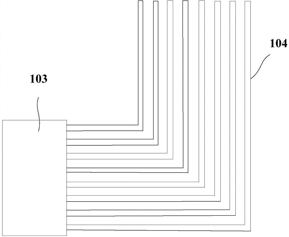
[0050] Please refer to Figure 4 , Figure 4 It is a schematic diagram of the arrangement structure of the signal connection line in Embodiment 1 of the present invention.

[0051]In this embodiment, the signal connection line includes a first connection line (not shown in the figure) and a second connection line 201, wherein the second connection line 201 is divided into two layers, and an insulating layer is arranged between the two layers of the second connection line 201 202. The area of ​​the array substrate occupied by the second connecting wires 201 on the upper layer is A1, the area of ​​the array substrate occupied by the second connecting wires 201 on the lower layer is A2, and the area A1 and the area A2 have an overlapping area A3.

[0052] Due to the overlapping area A3, when the number, width, and spacing of the second connecting lines are the same, the width of the non-display area of ​​the array substrate occupied by the second connecting lines distributed on ...

Embodiment 2

[0054] Please refer to Figure 5 , Figure 5 It is a schematic diagram of the arrangement structure of the signal connection line in Embodiment 2 of the present invention.

[0055] In this embodiment, the signal connection line includes a first connection line (not shown in the figure) and a second connection line 201, wherein the second connection line 201 is divided into two layers, and an insulating layer is arranged between the two layers of the second connection line 201 202, the area of ​​the array substrate occupied by the second connecting wires 201 on the upper layer is A1, the area of ​​the array substrate occupied by the second connecting wires 201 on the lower layer is A2, and the area A1 and the area A2 have an overlapping area A4.

[0056] Due to the overlapping area A4, when the number, width, and spacing of the second connecting lines are the same, the width of the non-display area of ​​the array substrate occupied by the second connecting lines distributed on...

Embodiment 3

[0058] Please refer to Image 6 , Image 6 It is a schematic diagram of the arrangement structure of the signal connection line according to the third embodiment of the present invention.

[0059] In this embodiment, the signal connection line includes a first connection line (not shown in the figure) and a second connection line 201, wherein the second connection line 201 is divided into two layers, and an insulating layer is provided between the two layers of the second connection line 201 Layer 202, the area of ​​the array substrate occupied by the second connecting wire 201 located on the upper layer is A1, the area of ​​the array substrate occupied by the second connecting wire 201 located on the lower layer is A2, the area A1 and the area A2 completely overlap, and the upper and lower sides The second connection lines 201 of the layers are overlapped.

[0060] Due to the completely overlapping area, when the number, width, and spacing of the second connecting lines are...


PUM


Abstract

The invention provides an array substrate, a manufacturing method of the array substrate and a display device. The array substrate comprises a display region, a non-display region and a plurality of signal connection wires, wherein the signal connection wires are located at the non-display region and used for being connected with a driving unit and comprise the first connection wires and the second connection wires, the first connection wires are electrically connected with the driving unit, the second connection wires are electrically connected with the first connection wires, the second connection wires are arranged in at least two layers, and each layer of the second connection wires is insulated from another layer of the second connection wires. By the adoption of the array substrate, the manufacturing method of the array substrate and the display device, the width of the part, occurred by the signal connection wires, of the non-display region of the array substrate can be reduced, and therefore the signal connection wires can be covered with silicon gel as much as possible, the risk of damage to the signal connection wires is reduced, the utilization rate of the array substrate can be increased, and the array substrate can be applied to the narrow bezel screen technology.

Description

technical field [0001] The present invention relates to the field of display technology, in particular to an array substrate, a manufacturing method thereof, and a display device. Background technique [0002] Please refer to figure 1 , figure 1 It is a structural schematic diagram of a thin film transistor (TFT) liquid crystal display panel in the prior art. The TFT liquid crystal display panel is mainly composed of a TFT array substrate 101 and a color filter (CF) substrate 102 . Please refer to figure 2 , figure 2 for figure 1 A schematic cross-sectional view of a TFT liquid crystal display panel in . After the cutting process (Cutting) is completed, the TFT array substrate 101 will be slightly larger than the CF substrate 102, and the larger part of the TFT array substrate 101 is used to set the chip-on-film (COF). The COF is the driver chip 103 (Driver IC, gate driver chip and source driver chip) carrier. In order to perform signal transmission between the dri...

Claims


Application Information

Patent Timeline
IPC IPC(8): G02F1/1362G02F1/1368G02F1/1333H01L27/12H01L21/77
CPCG02F1/1345G02F1/13458H01L2924/0002H01L27/124H01L2924/00H01L23/3171
Inventor 田川徐伟王勇李国红
Owner BOE TECH GRP CO LTD
Why Eureka
Try Eureka