Exposure device and exposure method

A technology of exposure device and spatial light modulator, applied in the direction of photolithography process exposure device, microlithography exposure equipment, etc., can solve the problem of difficulty in increasing the power of pulsed laser, reduce the overall display time, improve the effective refresh rate, The effect of increasing productivity

Active Publication Date: 2014-07-02
SHANGHAI MICRO ELECTRONICS EQUIP (GRP) CO LTD
View PDF8 Cites 7 Cited by
  • Summary
  • Abstract
  • Description
  • Claims
  • Application Information

AI Technical Summary

Problems solved by technology

However, it is difficult to increase the power of pulsed lasers. As the substrate area increases, the problem of light source energy will become more prominent

Method used


Image

  • Exposure device and exposure method
  • Exposure device and exposure method
  • Exposure device and exposure method

Examples


Embodiment 1

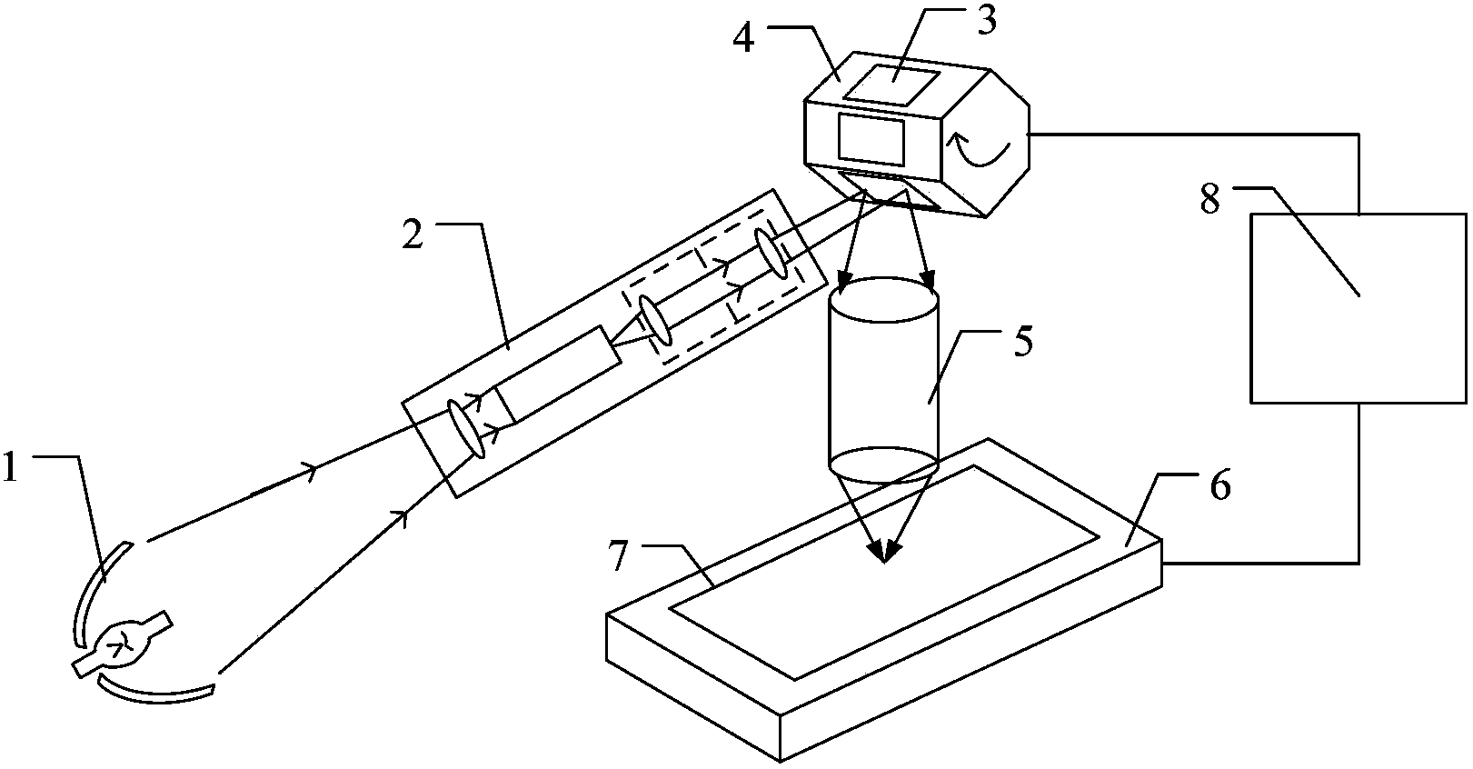
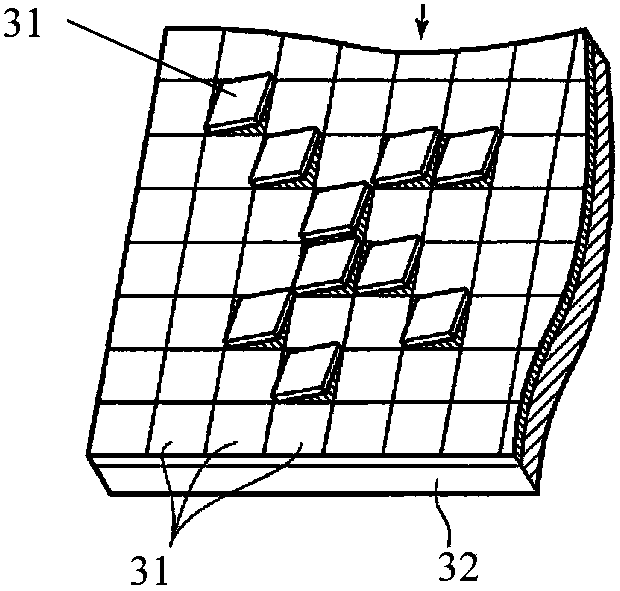
[0037] see figure 1, the exposure device provided in this embodiment is used to expose the glue-coated substrate 7 at least twice, including a light source 1, an illumination unit 2, at least two spatial light modulators 3, a motion mechanism 4, a projection objective lens 5, and a workpiece table 6 And a control unit 8, the at least two spatial light modulators 3 are installed on the motion mechanism 4 respectively, and the spatial light modulator 3, the motion mechanism 4 and the workpiece table 6 are respectively controlled by the control unit 8 control, the workpiece table 6 carrying the glue-coated substrate 7 moves to the position to be exposed under the control of the control unit 8, and the movement mechanism 4 moves the at least The two spatial light modulators 3 are sequentially adjusted to the object plane of the projection objective lens 5 for exposure, and each spatial light modulator 3 sequentially performs the data loading stage (that is, the Load state) and dev...

Embodiment 2

[0060] see Figure 7 The difference between this embodiment and Embodiment 1 is that: the moving mechanism 4 is a planar structure, and the at least two spatial light modulators 3 are arranged on the planar structure at intervals along the scanning direction. In this embodiment, the spatial light modulator 3 is a DMD, and the number of DMDs is two, which are DMD1 and DMD2, and of course the number can be set as needed. When DMD1 was brought to the object plane of projection objective lens 5, DMD1 just finished in Reset state, and began to enter the graphic display stage, and DMD2 was in Load state; when DMD1 was taken away from the object plane of projection objective lens 5, DMD2 was brought into The object plane of the objective lens 5 is projected and is in the Reset state. Theoretically, the motion mechanism 4 can drive multiple DMDs to perform reciprocating motion. Since the graphic refresh time of a single DMD is distributed to two DMDs in space, the overall frame rate ...

Embodiment 3

[0062] see Figure 8 The difference between this embodiment and Embodiment 1 is that the motion mechanism 4 is a turntable structure, and the at least two spatial light modulators 3 are distributed on the turntable structure around the center of the turntable structure. Preferably, in the exposure device of this embodiment, the at least two spatial light modulators 3 are evenly distributed on the turntable structure around the center of the turntable structure.

[0063] In this embodiment, the spatial light modulator 3 is a DMD, and the number of DMDs is 4, specifically DMD1, DMD2, DMD3 and DMD4, which uniformly rotate around a fixed shaft located at the center of the turntable structure. When DMD1 was brought to the object plane of projection objective lens 5, DMD1 just in time completed in the Reset state, and began to enter the graphic display stage, and the follow-up graphics DMD2, DMD3, DMD4 were in the Load state, only to be rotated to effective positions, due to the sin...


PUM


Abstract

The invention relates to an exposure device used for carrying out exposure for a gluing base for at least two times. The exposure device comprises at least two SLMs (Spatial Light Modulators), a movement mechanism, a projection objective lens, a workbench, the gluing base and a control unit, wherein the at least two SLMs are respectively installed on the movement mechanism, the SLMs, the movement mechanism and the workbench are respectively controlled by the control unit, the workbench loaded with the gluing base moves to a position to be exposed under the control of the control unit, the movement mechanism sequentially adjusts the at least two SLMs to an object plane of the projection objective lens under the control of the control unit for exposure, each SLM sequentially carries out a data loading stage, a device resetting stage and a graphical display stage under the control of the control unit, the control unit controls all the SLMs to carry out any one of the stages simultaneously, so that the overall effective refresh rate of all the SLMs is increased, the production rate of maskless lithography equipment is increased, and the display time of SLM graphs is shortened. High-resolution graphs can be made by using a continuous light source.

Description

technical field [0001] The invention relates to the field of semiconductor photolithography, in particular to an exposure device and an exposure method. Background technique [0002] The projection exposure device can project the circuit pattern on the reticle onto the substrate coated with photosensitive adhesive at a certain magnification or reduction ratio through an optical system such as a projection objective lens. At present, projection exposure devices have been widely used in the manufacture of integrated circuits, and in recent years, the scope of application has been extended to fields such as flat panel display and printed circuit board manufacturing. [0003] As the market demand for semiconductor products continues to increase and manufacturers continue to pursue their price competitiveness, the size of the initially processed flat panel display substrate and PCB substrate continues to increase. In the field of flat panel display, scanning projection exposure ...

Claims


Application Information

Patent Timeline
IPC IPC(8): G03F7/20
Inventor 许琦欣郑乐平
Owner SHANGHAI MICRO ELECTRONICS EQUIP (GRP) CO LTD
Why Eureka
Try Eureka