Screen printing identifying method for pins of device packaging libraries

A device packaging and pin technology, used in instruments, special data processing applications, electrical digital data processing, etc., can solve problems such as low efficiency and cumbersome operation, and achieve the effect of improving work efficiency, simple operation and reducing workload.

Active Publication Date: 2014-07-02
P C B A ELECTRONICS WUXI
View PDF4 Cites 19 Cited by
  • Summary
  • Abstract
  • Description
  • Claims
  • Application Information

AI Technical Summary

Problems solved by technology

However, none of the existing mainstream software has this function. Designers can only add labels to devices by placing them manually. It takes 3-4 minutes to add character labels to a 20x20pins BGA device, and add silk screen labels to a 208pin QFP device. It takes 2-3 minutes, and it takes 2-3 minutes to add a character mark to an LRM connector, which is cumbersome and inefficient

Method used


Image

  • Screen printing identifying method for pins of device packaging libraries

Examples


Embodiment Construction

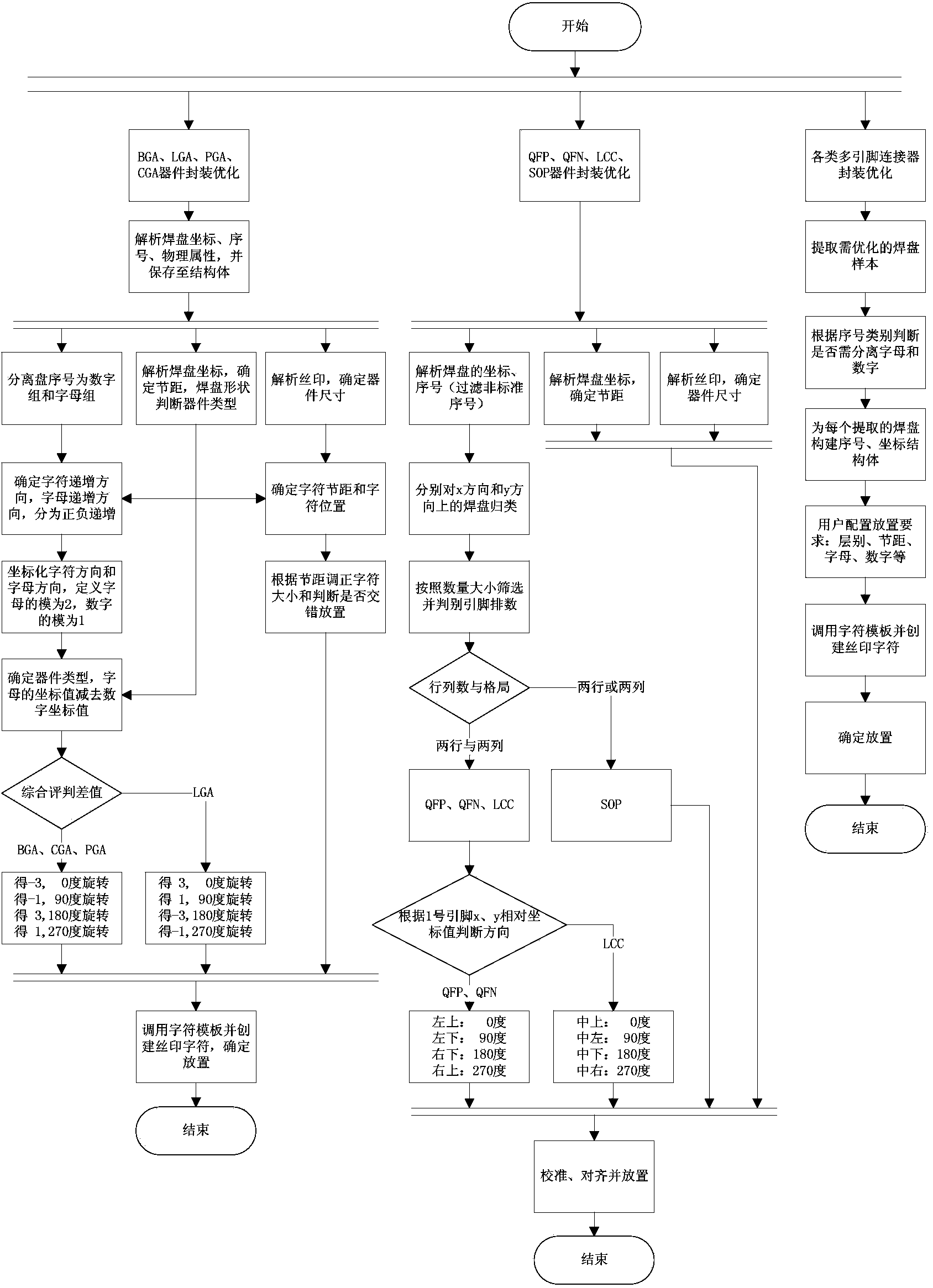
[0041] The present invention will be further described below in conjunction with drawings and embodiments. It should be understood that the specific embodiments described here are only used to explain the present invention, but not to limit the present invention. In addition, it should be noted that, for the convenience of description, only parts related to the present invention are shown in the drawings but not all content.

[0042] Please refer to figure 1 as shown, figure 1 It is a flow chart of a method for silk screen identification of pins in a device package library provided by an embodiment of the present invention.

[0043] In this embodiment, the method for silk screen identification of the pins of the device packaging library specifically includes the following steps: 1. Distinguish the type of device by extracting the characteristic information of different types of devices; 2. For each type of device, extract the pin serial number, pad type, Pad size, pad coord...


PUM


Abstract

The invention discloses a screen printing identifying method for pins of device packaging libraries. The screen printing identifying method includes steps of extracting feature information of different types of devices and judging the types of the devices; extracting sequence numbers of the pins, types of bonding pads, the sizes of the bonding pads and coordinates of the bonding pads for each type of devices; judging various directions, pitches, sizes and pin sequences of the devices and converting the directions, the pitches, the sizes and the pin sequences of the devices into positions, directions and properties of required screen printing identities. The screen printing identifying method has the advantages that the identities can be quickly added, operation is simple, the accuracy and the efficiency are high, durations for creating and optimizing integrated chip packaging libraries and connector packaging libraries can be greatly shortened for the PCB (printed circuit board) industry, the work efficiency of management personnel of the packaging libraries can be improved, and work burden on the management personnel can be relieved.

Description

technical field [0001] The invention relates to the technical field of silk screen marking, in particular to a method for silk screen marking of pins in a device packaging library. Background technique [0002] In the era of highly integrated technology and the development of distributed computing, integrated chips and multi-pin high-speed connectors are used more and more frequently. In the PCB (printed circuit board) industry, the creation of integrated chip package libraries and connector package libraries The time spent on optimization and optimization is no longer a small amount. It has become a customary rule to add silk screen marks to integrated device packages and connector packages. The role of silk screen marks in PCB design, PCB inspection, device soldering, and hardware debugging cannot be ignored. However, none of the existing mainstream software has this function. Designers can only add labels to devices by placing them manually. It takes 3-4 minutes to add ch...

Claims


Application Information

Patent Timeline
Patent Type & Authority Applications(China)
IPC IPC(8): G06F17/50
Inventor 应朝晖陈传开王永康王锡刚陈懿刘鹍
Owner P C B A ELECTRONICS WUXI
Why Eureka
Try Eureka