Unlock instant, AI-driven research and patent intelligence for your innovation.

A kind of array substrate and its preparation method, liquid crystal display panel

An array substrate and substrate technology, which is applied in the field of flat panel display, can solve the problems of high preparation cost and complicated preparation process, and achieve the effect of reducing the preparation cost and simplifying the preparation process.

Active Publication Date: 2016-10-19
SHANGHAI TIANMA MICRO ELECTRONICS CO LTD +1
View PDF4 Cites 0 Cited by
  • Summary
  • Abstract
  • Description
  • Claims
  • Application Information

AI Technical Summary

Problems solved by technology

[0013] To sum up, the existing technology needs to use 6 masks to realize the preparation of the array substrate, the preparation process is relatively complicated, and the preparation cost is relatively high

Method used


Image

  • A kind of array substrate and its preparation method, liquid crystal display panel
  • A kind of array substrate and its preparation method, liquid crystal display panel
  • A kind of array substrate and its preparation method, liquid crystal display panel

Examples


Embodiment 1

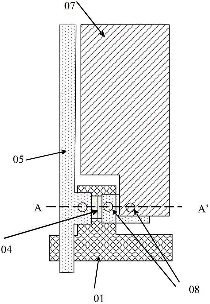
[0037] Embodiment 1 of the present invention provides an array substrate, and the schematic structural diagram of the pixel region of the array substrate can be as follows image 3 as shown, Figure 4 for image 3 The cross-sectional schematic diagram of the position of AA' in the middle, combined with the following image 3 and Figure 4 The array substrate provided in this embodiment will be described.

[0038] In this embodiment, the array substrate includes a TFT, and the TFT includes a substrate 11, and a gate 12, a gate insulating layer 13, an oxide semiconductor layer 14, an etching stopper layer 15, and a passivation layer formed sequentially on the substrate. layer 17 and pixel transparent conductive oxide layer 19.

[0039] The substrate 11 can be a transparent substrate, preferably, the substrate 11 can be a transparent glass substrate; the gate 12 can be used to load scanning signals to control the conduction or non-conduction of the oxide semiconductor layer 1...

Embodiment 2

[0058] Embodiment 2 of the present invention provides a method for preparing an array substrate, and the method may include the following steps:

[0059] The first step is to form the gate and the first conductive layer.

[0060] In this step, a metal thin film may be deposited on the substrate 11 , and the gate 12 and the first conductive layer 20 are photoetched on the metal thin film by using a first mask. So far, the gate 12 and the first conductive layer 20 have been formed by using the first mask.

[0061] The second step is to form a gate insulating layer.

[0062] In this step, a gate insulating layer 13 may be deposited and formed on the gate 12 and the substrate 11 . The array substrate formed at this time may be as shown in FIG. 5( a ).

[0063] The third step is to form an oxide semiconductor layer.

[0064] In this step, an oxide semiconductor film can be deposited on the gate insulating layer 13, and a pattern is etched on the oxide semiconductor film by usin...


PUM


Abstract

An embodiment of the invention provides an array substrate, a preparation method thereof and a liquid crystal display panel. Through holes allowing source drain regions of an oxide semiconductor layer to be exposed are not formed when a corrosion blocking layer is formed, but formed when a passivation layer is formed, therefore, a pixel transparent conductive oxide layer is deposited in the through holes and contacts with the source drain regions to form source drains, and one of the source drain regions is connected with the pixel transparent conductive oxide layer of a pixel region. Accordingly, during preparation of the array substrate, the quantity of masks required when the through holes are photo-etched out in the corrosion blocking layer are decreased, the preparation process of the array substrate is simplified, and preparation cost is reduced.

Description

technical field [0001] The invention relates to the field of flat panel display technology, in particular to an array substrate, a preparation method thereof, and a liquid crystal display panel. Background technique [0002] At present, in the technology of using an oxide thin film field effect transistor (Thin Film Transistor, TFT) to drive a twisted nematic liquid crystal display (Twisted Nematic Liquid Crystal Display, TN-LCD), until the formation of the pixel indium tin oxide layer (Pixel ITO layer ), the preparation process of the array substrate needs to use 6 masks (Mask). Use Mask1, Mask2, Mask3, Mask4, Mask5 and Mask6 to represent 6 Masks respectively, and the preparation process of the array substrate may specifically include the following steps: [0003] The first step is to deposit a metal thin film on a transparent substrate, and use Mask1 to etch a gate on the metal thin film. [0004] The second step is to form a gate insulating layer. [0005] The third st...

Claims


Application Information

Patent Timeline
Patent Type & Authority Patents(China)
IPC IPC(8): H01L27/12H01L29/786H01L21/77G03F7/00G02F1/1333
Inventor 楼均辉
Owner SHANGHAI TIANMA MICRO ELECTRONICS CO LTD