Oxide thin film transistor structure and method for producing same

A technology for oxide thin films and transistors, applied in transistors, semiconductor/solid-state device manufacturing, semiconductor devices, etc., can solve problems such as affecting the electrical properties of the metal oxide layer 104, disconnection, etc.

Inactive Publication Date: 2014-07-09
HANNSTAR DISPLAY CORPORATION
View PDF5 Cites 5 Cited by
  • Summary
  • Abstract
  • Description
  • Claims
  • Application Information

AI Technical Summary

Problems solved by technology

However, it is known that the metal oxide layer 104 below the source 105 and the drain 106 is often corroded by the metal etchant when the lithographic etching process of the source 105 and the drain 106 is performed on t

Method used


Image

  • Oxide thin film transistor structure and method for producing same
  • Oxide thin film transistor structure and method for producing same
  • Oxide thin film transistor structure and method for producing same

Examples


Embodiment Construction

[0053]The following is a detailed description of preferred embodiments of the present invention with the accompanying drawings. The following description and drawings use the same reference numerals to indicate the same or similar elements, and repeated descriptions of the same or similar elements are omitted.

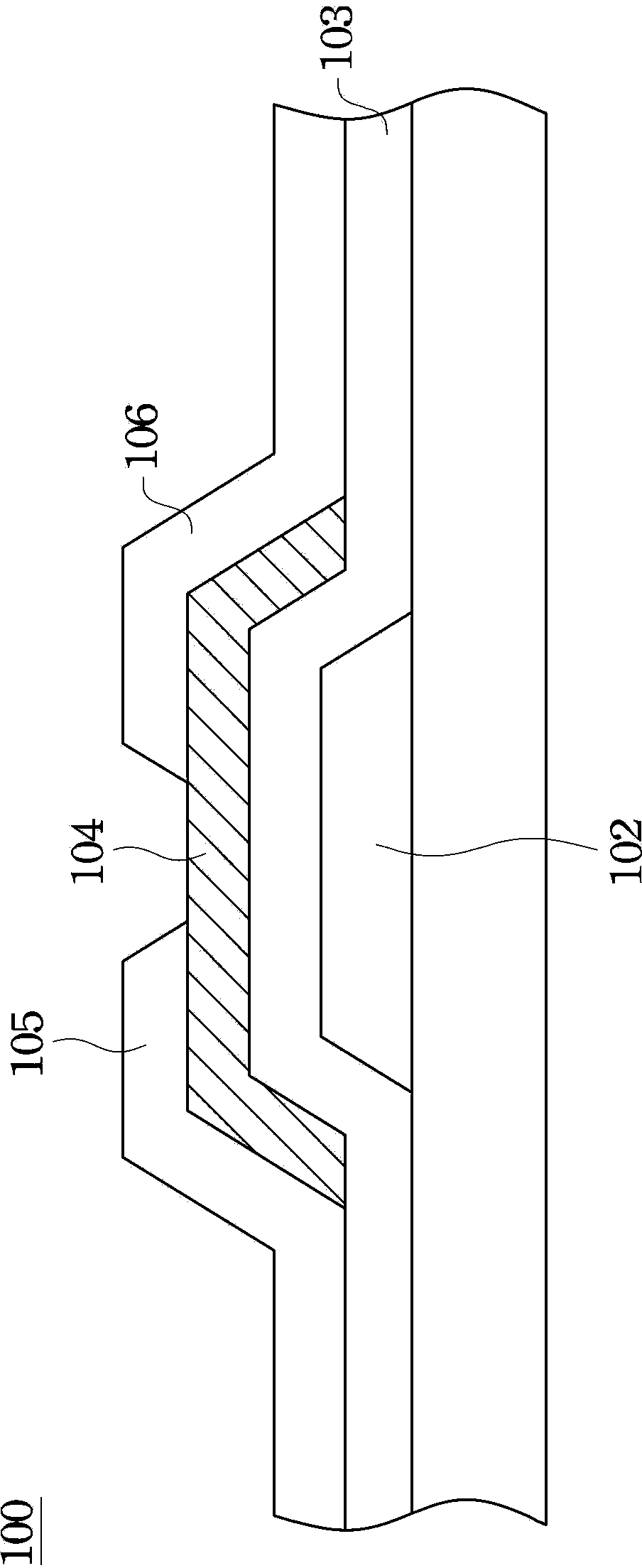
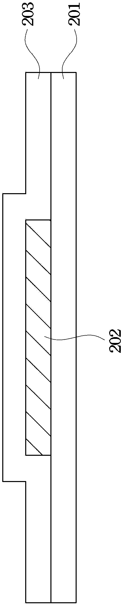
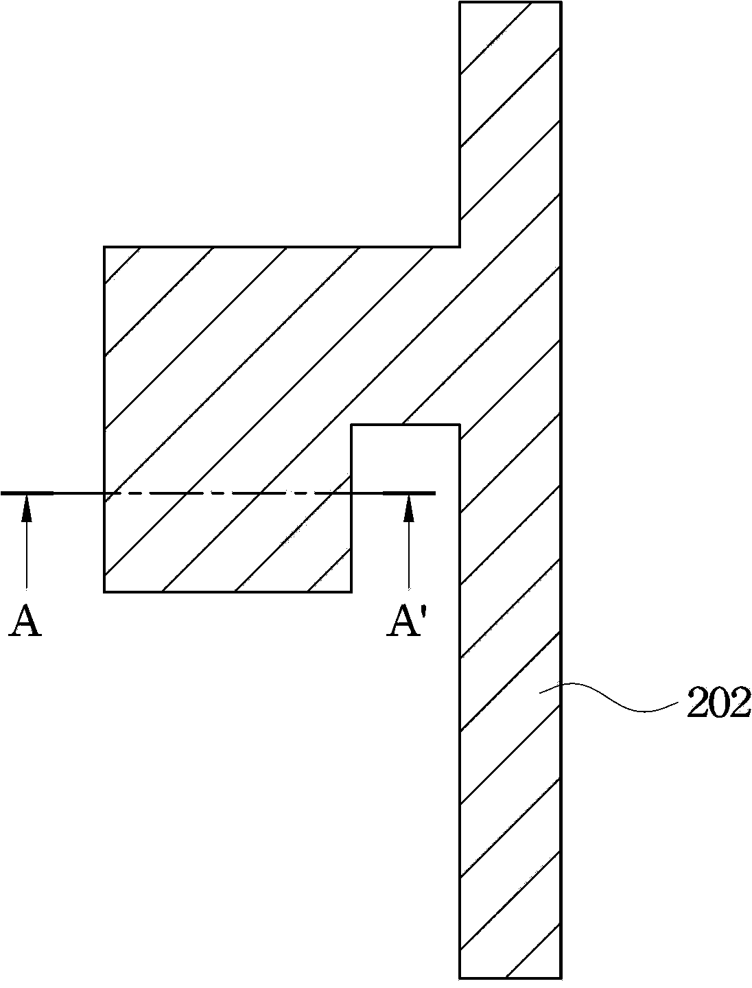
[0054] Please refer to Figure 8A , Figure 8A A schematic cross-sectional view showing the structure of an oxide thin film transistor according to a preferred embodiment of the present invention. Such as Figure 8A As shown, the oxide TFT structure 200 of this embodiment includes a substrate 201 . A drain 202 is disposed on the substrate 201 . A first insulating layer 203 is disposed on the substrate 201 and the drain 202 , and an opening 203 a is disposed on the first insulating layer 203 to expose part of the surface of the drain 202 . A gate 204 and a gate insulating layer 205 are sequentially disposed on the first insulating layer 203 and disposed on a side of...


PUM


Abstract

The invention discloses an oxide thin film transistor and a method for producing same. The oxide thin film transistor structure comprises a substrate, and a drain electrode is disposed on the substrate. A first insulating layer is disposed on the substrate and the drain electrode. A drain electrode surface having a first opening so as to be partially exposed is disposed on the first insulating layer. A gate electrode and a gate insulating layer are sequentially disposed on the first insulating layer and on two sides of the first opening. A metal oxide channel layer is disposed on the gate insulating layer and in the first opening. A source electrode is disposed on the metal oxide channel layer. The corresponding position in the metal oxide channel layer to the first opening is taken as a channel region.

Description

technical field [0001] The present invention relates to a transistor structure and a manufacturing method thereof, in particular to a structure of an oxide thin film transistor and a manufacturing method thereof. Background technique [0002] In recent years, flat panel displays have developed more and more rapidly, and have gradually replaced traditional cathode ray tube displays. Today's flat panel displays mainly include the following types: Organic Light-Emitting Diodes Display (OLED), Plasma Display Panel (PDP), Liquid Crystal Display (LCD), and Field Emission Display (Field Emission Display). Display, FED), etc. The thin film transistor (Thin Film Transistor, TFT), which controls the on and off of each pixel in these flat panel displays, is one of the key elements in these flat panel displays. [0003] figure 1 A schematic cross-sectional view of a known metal oxide thin film transistor structure is shown. Such as figure 1 As shown, the known metal oxide thin film...

Claims


Application Information

Patent Timeline
IPC IPC(8): H01L29/786H01L29/417H01L29/423H01L29/10H01L21/336H01L21/28
CPCH01L29/66969H01L29/7869H01L29/78696
Inventor 张民杰
Owner HANNSTAR DISPLAY CORPORATION
Why Eureka
Try Eureka