Touch panel, manufacturing method thereof and touch display device

A touch panel and touch sensing technology, applied in the direction of instruments, adhesive types, adhesives, etc., can solve the problems of high energy consumption, etc., and achieve the effects of enhanced induction current, good touch effect, and improved sensitivity

Active Publication Date: 2014-07-23
WUHAN TIANMA MICRO ELECTRONICS CO LTD +1
View PDF3 Cites 1 Cited by
  • Summary
  • Abstract
  • Description
  • Claims
  • Application Information

AI Technical Summary

Problems solved by technology

[0005] The purpose of the present invention is to provide a touch panel and its manufacturing method and a touch display device to solve the problem of the need to enhance the power consumption signal to obtain a better touch effect when determining the touch position of the existing touch panel. bigger problem

Method used


Image

  • Touch panel, manufacturing method thereof and touch display device
  • Touch panel, manufacturing method thereof and touch display device
  • Touch panel, manufacturing method thereof and touch display device

Examples


Embodiment Construction

[0020] The following will clearly and completely describe the technical solutions in the embodiments of the present invention in conjunction with the accompanying drawings in the embodiments of the present invention. Obviously, the described embodiments are only some of the embodiments of the present invention, not all of them. Based on the embodiments of the present invention, all other embodiments obtained by persons of ordinary skill in the art without making creative efforts belong to the protection scope of the present invention.

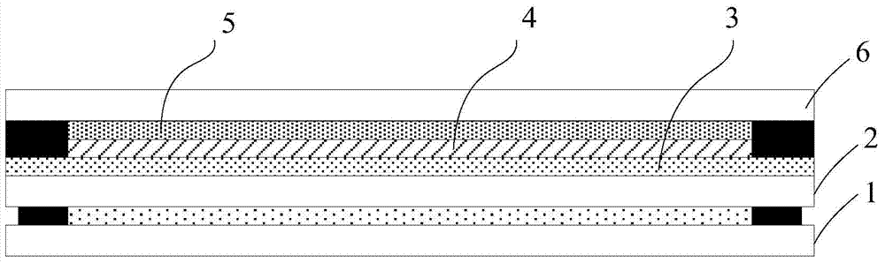
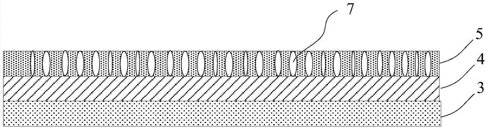
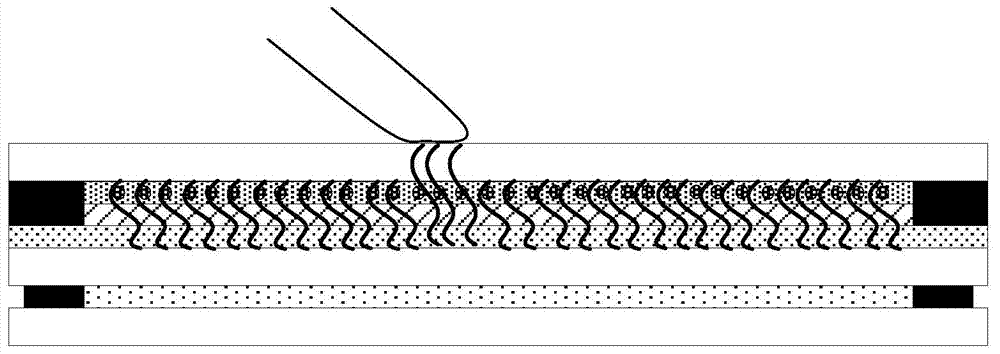
[0021] An embodiment of the present invention provides a touch panel, figure 2 Shown is a schematic cross-sectional structure diagram of the touch panel provided by the embodiment of the present invention, as figure 2 As shown, the touch panel provided by the embodiment of the present invention includes a touch sensing layer 3 and an insulating layer 4 thereon, and also includes an adhesive layer 5 arranged on the insulating layer 4, and the ...


PUM


Abstract

The invention discloses a touch panel, a manufacturing method of the touch panel and a touch display device. The touch panel comprises a touch induction layer, an insulating layer located on the touch induction layer and a glue layer arranged on the insulating layer. The glue layer is doped with conductive materials at the set ratio. According to the touch panel, the glue layer located on the insulating layer comprises the conductive materials, wherein the glue layer is doped with the conductive materials, electrical conductivity of the glue layer is enhanced, the induction current generated by the human body is enhanced, capacity for forming coupling capacitance between the human body and the touch induction layer is improved, good induction capacity is achieved, touch induction sensitivity can be improved, and the good touch effect is achieved.

Description

technical field [0001] The present invention relates to the field of touch technology, in particular to a touch panel, a manufacturing method thereof, and a touch display device. Background technique [0002] With the development of touch technology, touch panels are more and more widely used. [0003] figure 1 Shown is a schematic cross-sectional structure diagram of a touch display device including a touch panel in the prior art, such as figure 1 As shown, the touch display device includes an array substrate 1 , a color filter substrate 2 , a touch sensing layer 3 , an insulating layer 4 , an adhesive layer 5 and a glass cover 6 . [0004] However by figure 1 It can be seen that the touch sensing layer 3 of the existing touch panel is provided with an insulating layer 4, an adhesive layer 5 and a glass cover 6, and the insulating layer 4, the adhesive layer 5 and the glass cover 6 form an isolated insulating area. The existence of the isolated insulating area weakens t...

Claims


Application Information

Patent Timeline
Patent Type & Authority Applications(China)
IPC IPC(8): G06F3/044C09J9/02C09J163/00
Inventor 李玉军赵本刚
Owner WUHAN TIANMA MICRO ELECTRONICS CO LTD
Why Eureka
Try Eureka