
Static random access memory and bit line pre-charging self-timing circuit thereof

A pre-charging circuit, static random technology, applied in the direction of static memory, digital memory information, information storage, etc., can solve the problems of static memory read and write access time and the impact of the minimum clock cycle, to achieve good resistance, good process voltage temperature deviation Effect

Active Publication Date: 2014-07-23
XI AN UNIIC SEMICON CO LTD
View PDF4 Cites 11 Cited by
  • Summary
  • Abstract
  • Description
  • Claims
  • Application Information

AI Technical Summary

Problems solved by technology

[0008] like figure 2 As shown, the traditional precharge signal based on the inverter chain delay is sensitive to the process voltage temperature (PVT) environment, so it is necessary to leave a lot of margin in the design, the read and write access time of the static memory and the minimum The clock period will have a negative impact on

Method used


Image

  • Static random access memory and bit line pre-charging self-timing circuit thereof
  • Static random access memory and bit line pre-charging self-timing circuit thereof
  • Static random access memory and bit line pre-charging self-timing circuit thereof

Examples


Embodiment Construction

[0036] Embodiments of the present invention will be further described below in conjunction with the accompanying drawings.

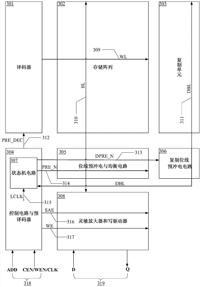
[0037] Such as image 3 as shown, image 3 It is an example of a SRAM implemented according to the present invention. The SRAM includes a decoder 301, a memory array 302, a copy unit 303, a control circuit and a pre-decoder 304, a bit line precharge and equalization circuit 305, a copy bit line precharge circuit 306, a state machine circuit 307 and a sensitive amplifier and write driver 308 .

[0038] The decoder 301 is connected to the memory array 302 through a plurality of word lines (WL) 309 , and the decoder 301 is also connected to the control circuit and the pre-decoder 304 through a plurality of pre-decoder outputs (PRE_DEC) 312 .

[0039] The memory array 302 is also connected to a bit line precharge and equalization circuit 305 and a sense amplifier and write driver 308 through a plurality of bit lines (BL) 310 .

[0040] The duplicate unit...


PUM


Abstract

The invention provides a static random access memory and a bit line pre-charging self-timing circuit thereof. A duplication unit is used for simulating load on a normal bit line; a duplication bit line pre-charging circuit is used for simulating a pre-charging circuit of the normal bit line and pre-charging and resetting a duplication bit line; a state machine circuit is used for controlling conversion between beginning and ending states of duplication bit-line pre-charging operations and producing self-timing signals for normal bit-line pre-charging operations. The circuit simulates the pre-charging process of the normal bit line so as to provide accurate self-timing for bit-line pre-charging operations of the static random access memory at different process voltage temperatures. Compared with a traditional method for generating a bit-line pre-charging signal in a delay mode based on a phase inverter chain, the circuit has excellent capability of resisting deviation of process voltage temperature.

Description

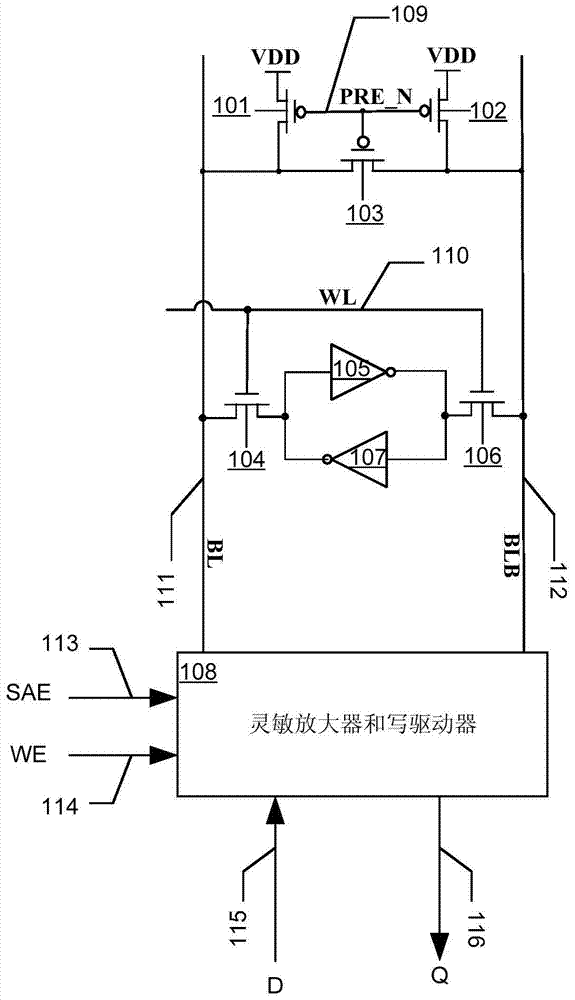
【Technical field】 [0001] The invention relates to the field of static random access memory design, in particular to a static random access memory and a bit line precharge self-timing circuit thereof. 【Background technique】 [0002] According to the forecast of the International Semiconductor Technology Roadmap (ITRS), the area of ​​the SRAM will become larger and larger, and by 2015, it will account for more than 94% of the area of ​​the entire system-on-chip (SOC). With the continuous evolution of process technology and the continuous shrinking of the size of semiconductor devices, local and global process deviations have an increasing impact on the performance and reliability of integrated circuits. [0003] see figure 1 as shown, figure 1 It is a schematic diagram of a typical SRAM data path. The typical datapath includes bit line precharge and equalization circuits, memory cells, sense amplifiers and write drivers. [0004] The pre-charging and equalizing circuit is ...

Claims


Application Information

Patent Timeline
IPC IPC(8): G11C11/413
Inventor 熊保玉拜福君
Owner XI AN UNIIC SEMICON CO LTD
Learn More