Grooved semiconductor device and manufacturing method thereof

A technology of semiconductors and conductive semiconductors, applied in semiconductor/solid-state device manufacturing, semiconductor devices, electrical components, etc., can solve problems such as high forward voltage drop

Inactive Publication Date: 2014-07-23
朱江
View PDF6 Cites 0 Cited by
  • Summary
  • Abstract
  • Description
  • Claims
  • Application Information

AI Technical Summary

Problems solved by technology

[0003] For traditional semiconductor devices, the on-resistance and turn-on voltage drop rise rapidly with the i...

Method used


Image

  • Grooved semiconductor device and manufacturing method thereof
  • Grooved semiconductor device and manufacturing method thereof
  • Grooved semiconductor device and manufacturing method thereof

Examples


Embodiment 1

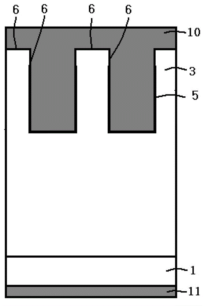
[0027] figure 1 It is a sectional view of a trench semiconductor device of the present invention, combined below figure 1 The semiconductor device of the present invention will be described in detail.

[0028] A trench semiconductor device, comprising: a substrate layer 1, which is an N conductivity type semiconductor silicon material, and the doping concentration of phosphorus atoms is 1E19 / CM 3 , on the lower surface of the substrate layer 1, the electrodes are drawn out through the lower surface metal layer 11; the first conductive semiconductor material 3, located on the substrate layer 1, is a semiconductor silicon material of N conductivity type, and the doping concentration of phosphorus atoms is 1E16 / CM 3 , there is a region doped with a high concentration of impurities near its upper surface; Schottky barrier junction 5, located on the inner wall of the trench, is a silicide formed by semiconductor silicon material and barrier metal, and the trench spacing is 0.5um; ...

Embodiment 2

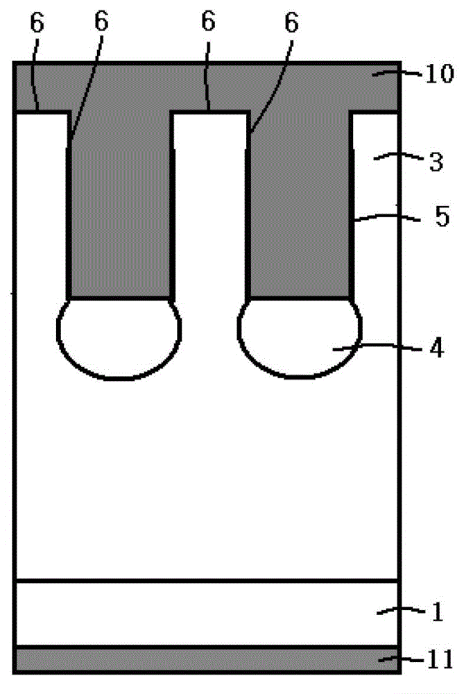
[0039] Figure 5 It is a sectional view of a trench semiconductor device of the present invention, combined below Figure 5 The semiconductor device of the present invention will be described in detail.

[0040] A trench semiconductor device, comprising: a substrate layer 1, which is an N conductivity type semiconductor silicon material, and the doping concentration of phosphorus atoms is 1E19 / CM 3 , on the lower surface of the substrate layer 1, the electrodes are drawn out through the lower surface metal layer 11; the first conductive semiconductor material 3, located on the substrate layer 1, is a semiconductor silicon material of N conductivity type, and the doping concentration of phosphorus atoms is 1E16 / CM 3 ; The second conductive semiconductor material 4, located in the inner wall region of the trench, is a semiconductor silicon material of P conductivity type, and the doping concentration of boron atoms is 1E16 / CM 3 , the groove pitch is 1um; the ohmic contact regi...


PUM

PropertyMeasurementUnit
Widthaaaaaaaaaa

Abstract

The invention discloses a grooved semiconductor device. When the semiconductor device is connected with a certain reverse bias voltage, depletion layers generated by semiconductor junctions on the inner walls of grooves are overlapped with one another, so that a conducting channel from a positive pole to a negative pole is shielded, and the semiconductor device has a reverse blocking function. Since materials with a charge compensation function are arranged at the bottoms of the grooves of the semiconductor device, the reverse blocking capability of the semiconductor device is improved. When the semiconductor device is connected with a certain forward bias voltage, the semiconductor device has an extremely low forward turn-on voltage drop since no semiconductor junction exists between the positive pole and the negative pole. The invention further provides a manufacturing method of the grooved semiconductor device.

Description

technical field [0001] The invention relates to a trench semiconductor device, and the invention also relates to a preparation method of the trench semiconductor device. The semiconductor device of the present invention is a basic structure for manufacturing power rectifying devices. Background technique [0002] Power semiconductor devices are widely used in power management and power applications. The most basic structure in power semiconductor devices is semiconductor junctions. Semiconductor junctions include PN junctions and Schottky barrier junctions; reduce the on-resistance and turn-on voltage of semiconductor junctions Power drop is an important trend in the development of power semiconductor devices. [0003] For traditional semiconductor devices, the on-resistance and turn-on voltage drop increase rapidly with the increase of the reverse blocking voltage of the device, which makes the device have a higher forward conduction voltage drop. Contents of the inventi...

Claims


Application Information

Patent Timeline
IPC IPC(8): H01L29/06H01L29/861H01L29/872H01L21/329
CPCH01L29/0615H01L29/66143H01L29/872
Inventor 朱江
Owner 朱江
Why Eureka
Try Eureka