Semiconductor device mixed with graphene electrode and manufacturing method of device

A technology of graphene electrodes and manufacturing methods, which is applied in the manufacture of semiconductor devices, electrical components, final products, etc., can solve the problems of weak signal detection ability, low metal light transmittance, small wavelength range, etc., and achieve strong detection of weak signals ability, high photoelectric conversion efficiency, and the effects of low reverse leakage current

Pending Publication Date: 2022-01-28
SOUTHEAST UNIV +1
View PDF5 Cites 2 Cited by
  • Summary
  • Abstract
  • Description
  • Claims
  • Application Information

AI Technical Summary

Problems solved by technology

However, there is only one kind of metal in direct contact with the surface of the epitaxial layer of the traditional Schottky diode. This metal has a unique work function, and the semiconductor can only produce a unique Schottky barrier, so the device has a small forward state. The two requirements of barrier height and having a large barrier height in the reverse state of the device are conflicting
In the field of optoelectronics, the traditional photodetector adopts a metal-semiconductor structure, the light transmittance of the metal is low, and the wavelength range of light that can be detected is small. At the same time, the photodetector with a low Schottky barrier has a large dark current and strong noise. The disadvantage of weak detection ability for weak signals

Method used


Image

  • Semiconductor device mixed with graphene electrode and manufacturing method of device
  • Semiconductor device mixed with graphene electrode and manufacturing method of device
  • Semiconductor device mixed with graphene electrode and manufacturing method of device

Examples


Embodiment 1

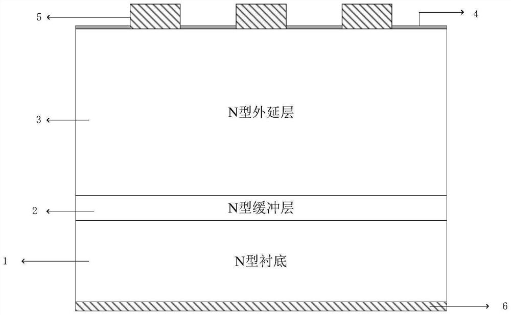
[0031] A kind of semiconductor device of mixed graphene electrode of the present invention comprises: N-type substrate 1, is provided with back electrode metal 6 on one surface of N-type substrate 1, is provided with on the other surface of N-type substrate 1 The N-type buffer layer 2 is provided with an N-type epitaxial layer 3 on the N-type buffer layer 2, and the surface of the N-type epitaxial layer 3 is provided with a graphene electrode 4 and a high work function metal forming a Schottky contact with the N-type epitaxial layer 3 Electrode 5.

[0032] The upper surface of the N-type epitaxial layer 3 is a plurality of protrusions, the graphene electrode 4 is located on the top of the protrusions, and the high work function metal electrode 5 is located on the side of the protrusions and the upper surface of the N-type epitaxial layer 3 .

[0033] The high work function metal electrode 5 is embedded in the upper surface of the N-type epitaxial layer 3, and the graphene elec...

Embodiment 2

[0042] The structure of the present invention is the same as embodiment 1, and the manufacture method of described structure:

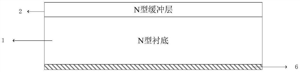
[0043] Step 1 as figure 2 As shown, take an N-type substrate 1, use a sputtering process, make a back electrode metal 6 on one surface of the N-type substrate 1, and grow an N-type buffer layer 2 on the other surface of the N-type substrate,

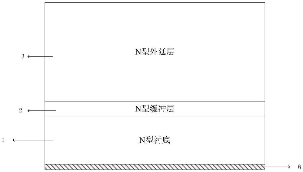
[0044] Step 2 as image 3 As shown, an N-type epitaxial layer 3 is formed on the surface of the N-type buffer layer 2,

[0045] Step 3 as Figure 4 As shown, the graphene is transferred to the surface of the N-type epitaxial layer 3 by using the transfer method, and then, using the plasma reactive etching technique, part of the graphene is etched away, leaving the graphene 4 distributed at intervals,

[0046] In step 4, a sputtering process and a metal lift-off process are used to form high work function metals 5 arranged at intervals in close contact with the graphene 4 on the N-type epitaxial layer 3 to fo...


PUM

PropertyMeasurementUnit
electron mobilityaaaaaaaaaa
electrical conductivityaaaaaaaaaa

Abstract

The invention relates to a semiconductor device mixed with a graphene electrode and a manufacturing method of the device. A cellular structure of the device comprises an N-type substrate, an N-type buffer layer, an N-type epitaxial layer, a graphene electrode and a metal electrode, wherein the surface of the graphene electrode and the surface of the metal electrode are in Schottky contact with the N-type epitaxial layer, and a metal back electrode in ohmic contact with the N-type substrate is arranged below the substrate. The device has the advantages that: the graphene has extremely high light transmittance and an adjustable work function, and the graphene and the metal with a relatively high work function form a mixed electrode on the surface of the N-type epitaxial layer, so that the dark current of the device is reduced, the noise is reduced, the sensitivity is improved, the weak signal detection capability is enhanced, the wavelength detection range is enlarged, and the performance stability is improved. The turn-on voltage of the device in a forward conduction state can be reduced, the leakage current in a blocking state can be reduced, and the breakdown voltage can be improved. The device can be applied to the photoelectric field and the power field.

Description

technical field [0001] The invention belongs to the field of semiconductor devices, in particular to a semiconductor device with mixed graphene electrodes and a manufacturing method thereof. Background technique [0002] The power dissipation of a Schottky diode depends on the forward voltage drop and reverse leakage current, both of which should be as low as possible to reduce the power dissipation of the device. In order to meet the forward voltage drop of the device, the height of the Schottky barrier needs to be low. In order to meet the low reverse leakage current of the device, the Schottky barrier should be as high as possible. However, there is only one kind of metal in direct contact with the surface of the epitaxial layer of the traditional Schottky diode. This metal has a unique work function, and the semiconductor can only produce a unique Schottky barrier, so the device has a small forward state. The two requirements of barrier height and having a large barrier...

Claims


Application Information

Patent Timeline
Patent Type & Authority Applications(China)
IPC IPC(8): H01L31/0224H01L31/108H01L31/18
CPCH01L31/022408H01L31/022466H01L31/108H01L31/18Y02P70/50
Inventor 魏家行徐航隗兆祥付浩薛璐洁王恒德刘斯扬孙伟锋时龙兴
Owner SOUTHEAST UNIV
Why Eureka
Try Eureka