
A method for collecting and processing ccd data

A technology of data collection and processing and data, which is applied in the direction of TV, color TV parts, electrical components, etc., can solve the problems of different responsiveness, etc., and achieve the effect of improving processing speed, improving data stability, and high data accuracy

Active Publication Date: 2017-06-06
FOCUSED PHOTONICS +1
View PDF5 Cites 0 Cited by
  • Summary
  • Abstract
  • Description
  • Claims
  • Application Information

AI Technical Summary

Problems solved by technology

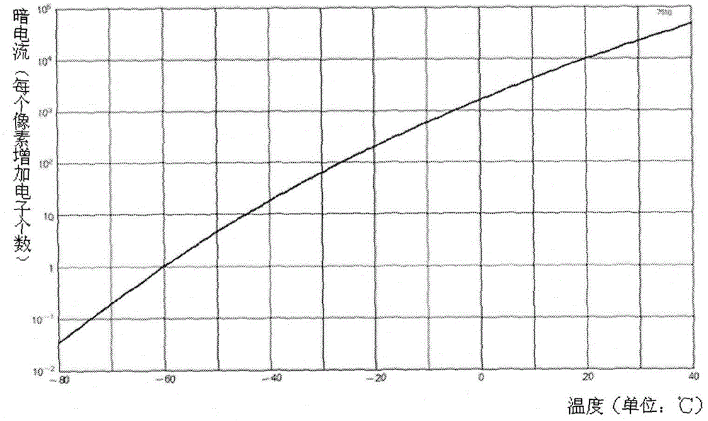
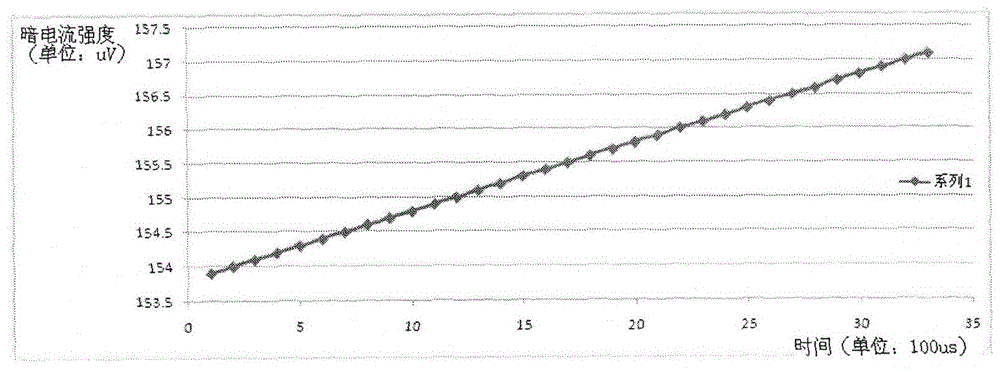
[0006] The area array CCD can also deduct the dark current by deducting the dumb pixels, but for different pixels, the responsivity is not the same, and there are certain fluctuations, so it is hoped to reduce the noise by deducting the dark current corresponding to the time of each pixel

Method used


Image

  • A method for collecting and processing ccd data
  • A method for collecting and processing ccd data
  • A method for collecting and processing ccd data

Examples


Embodiment 1

[0039] A method for collecting and processing CCD data, comprising the following steps:

[0040] A. Set the pre-exposure time t, open the shutter, and perform pre-exposure;

[0041] B. Drive the CCD, collect the pre-exposure signals of each effective area, obtain the optimal integration time required by each effective area, and then obtain the minimum integration unit time t of the CCD min ;

[0042] C. put t min Expose successively as the actual exposure time, and store the data after each exposure in the storage area according to the effective area:

[0043] complete once t min Integrate, perform CCD fast drive, read the signals of each effective area, and store the read signals of each effective area in the buffer space; and then perform the next t min After the integration is completed, the CCD is also driven to read the signals of each effective area, and accumulated and stored in the storage area of ​​the buffer space corresponding to each effective area; sequentiall...

Embodiment 2

[0070] This embodiment is an application example of Embodiment 1. In this application example, three effective areas are set, namely A 1 、A 2 and A 3 ;

[0071] A method for collecting and processing CCD data, comprising the following steps:

[0072] A. Set the pre-exposure time t100ms (fixed exposure time, which can be set according to specific needs), open the shutter, and perform pre-exposure;

[0073] B. Drive the CCD, collect the pre-exposure signals of each effective area, obtain the best integration time of each effective area, and then obtain the minimum integration unit time t of the CCD min :

[0074] Each of the effective areas corresponds to A 1 、A 2 and A 3 , the maximum light intensity signals corresponding to each effective area are I 1 , I 2 and I 3 , according to the set CCD optimal response light intensity I 0 , the optimal integration time of each effective area is obtained as t 1 =t*I 0 / I 1 , t 2 =t*I 0 / I 2 and t 3 =t*I 0 / I 3 , then t...


PUM


Abstract

The invention relates to a CCD data collecting and processing method. The method comprises the following steps: A, setting a pre-exposure time t, opening a shutter, and performing pre-exposure; B, driving a CCD, collecting pre-exposure signals of all the effective areas, obtaining the best integral time of all the effective areas, and then obtaining the minimum integral unit time tmin of the CCD; C, performing gradual exposure by enabling the tmin to serve as actual exposure time, and storing data after exposure of each time in storage areas in a corresponding accumulation mode according to the effective areas, wherein when the effectively areas reach the best integral time, the data corresponding to the storage areas are strength signals I corresponding to pixel points of all the areas. The method has the advantages of being short in total parsing time, high in data accuracy and the like.

Description

technical field [0001] The invention relates to a data collection and processing method, in particular to a CCD data collection and processing method. Background technique [0002] In various instruments and meters such as atomic emission spectrometers, array detectors such as CCDs and CMOSs ​​can achieve functions that traditional single sensors require hundreds or even tens of thousands of sensors because of their large number of pixels and high integration. is becoming increasingly widespread. [0003] However, in practical applications, the actual signal values ​​detected by different pixels in an array detector are different. In some areas, the signal is too small, the sensitivity is not enough, and the signal-to-noise ratio is not high, while the signal in some areas is saturated and cannot be used. [0004] In order to enable the entire array detector to collect effective data, it is necessary to integrate signals in different regions at different times. In this way...

Claims


Application Information

Patent Timeline
Patent Type & Authority Patents(China)
IPC IPC(8): H04N5/353H04N5/361
Inventor 夏晓峰俞晓峰吕全超寿淼钧
Owner FOCUSED PHOTONICS
Learn More