Wafer-level zoom lens module and production method thereof

A zoom lens, wafer-level technology, applied in nonlinear optics, instruments, optics, etc., to achieve the effect of convenient specification

Active Publication Date: 2014-08-06
HOWE OPTOELECTRONICS TECH SHANGHAI
View PDF7 Cites 5 Cited by
  • Summary
  • Abstract
  • Description
  • Claims
  • Application Information

AI Technical Summary

Problems solved by technology

[0006] The lens modules in the above two patents are lens modules

Method used


Image

  • Wafer-level zoom lens module and production method thereof
  • Wafer-level zoom lens module and production method thereof
  • Wafer-level zoom lens module and production method thereof

Examples


Embodiment 1

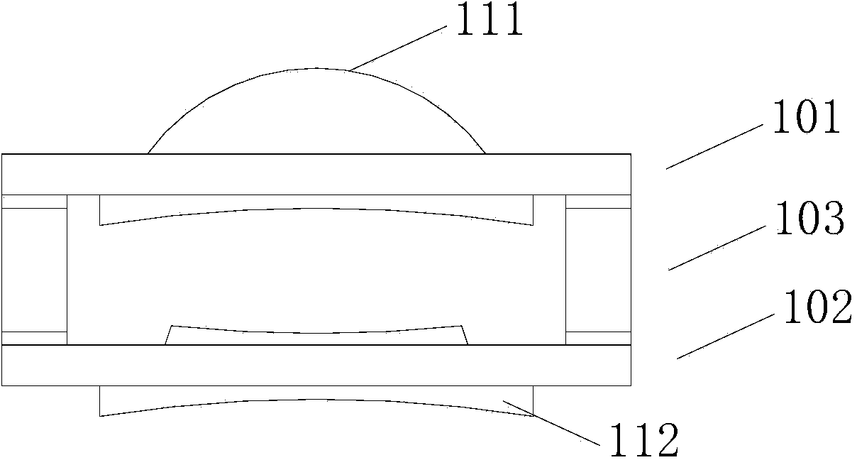
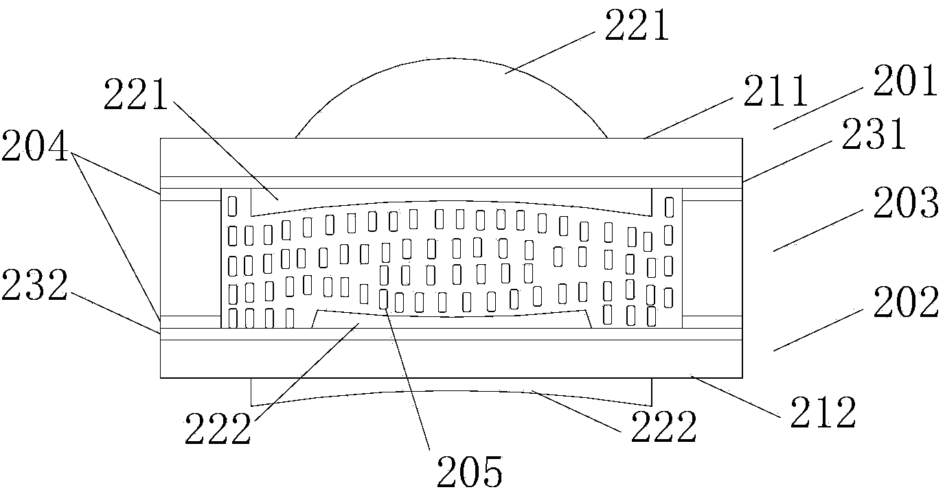
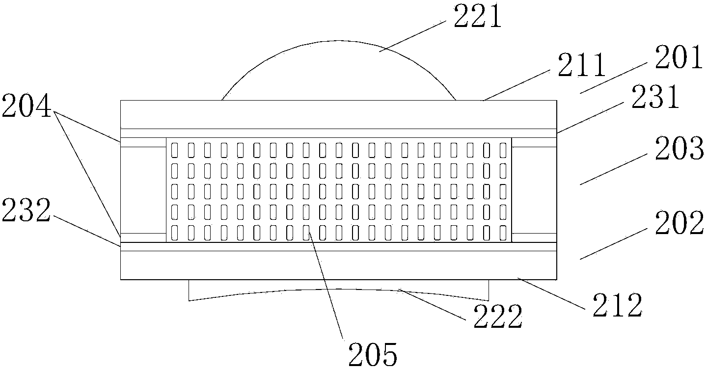
[0076] like Figure 2A-2B As shown, the wafer-level zoom lens module in this embodiment includes: a first lens layer 201 and a second lens layer 202 , and a spacer layer 203 located between the first lens layer 201 and the second lens layer 202 . The first lens layer 201 includes a first transparent conductive glass substrate 211, at least one first lens 221 and a first transparent conductive film 231; the second lens layer 202 includes a second transparent conductive glass substrate 212, at least one second lens 222 and the second transparent conductive film 232; one of the surfaces of the first transparent conductive glass substrate 211 is covered with the first transparent conductive film 231, similarly, one of the surfaces of the second transparent conductive glass substrate 212 is covered with the second transparent conductive film 232 . The first lens 221 and the second lens 222 are both plano-convex lenses or plano-concave lenses, that is, lenses with a plane surface a...

Embodiment 2

[0082] Because the wafer-level zoom lens module in the present invention is not limited to two layers of lens layers, it can also include three layers or more than three layers of lens layers. The structure of the lens module above the lens layer is roughly similar, therefore, in this embodiment, a lens module with three lens layers is taken as an example for detailed description.

[0083] like image 3 As shown, the wafer-level zoom lens module in this embodiment includes: a top wafer layer 301 at the top of the lens module, a middle lens layer 302 at the middle of the lens module, a bottom lens layer 303 at the bottom of the lens module and A plurality of spacer layers 301 located between every two adjacent lens layers. The arrangement of the top lens layer 301 and the bottom lens layer 303 is the same as that of the first lens layer 301 and the second lens layer 302 in Embodiment 1, so details will not be repeated here. The middle lens layer 302 in this embodiment include...


PUM

PropertyMeasurementUnit
Thicknessaaaaaaaaaa
Thicknessaaaaaaaaaa
Thicknessaaaaaaaaaa

Abstract

The invention provides a wafer-level zoom lens module and a production method thereof. A photo refraction material such as liquid crystal is filled in a cavity formed by two adjacent layers of lens sets and a gasket arranged between the two adjacent layers of lens sets, transparent conductive film is arranged in the two lens sets respectively and is connected with a changeable voltage source to be used as a pair of parallel potential plates, an electric field between the parallel potential plates can be formed, and the photo refraction materials generate a photoelectric effect under the action of the electric field to change the refractive index or the abbe number, accordingly, the whole optical lens module focus is changed, and variable focuses are achieved.

Description

technical field [0001] The invention relates to the field of zoom lens manufacturing, in particular to a wafer-level zoom lens module and a preparation method thereof. Background technique [0002] At present, the focal length of a general optical lens module is usually fixed, that is, after the lens module completes the corresponding manufacturing process and forms a corresponding product or sample, its own focal length cannot be further changed. Because the distance between different lens groups in the lens module is set to a fixed value, taking the lens module composed of two groups of chips as an example, as figure 1 As shown, its structure generally includes: a first lens group 101, a second chip group 102 and a spacer part 103; the first chip group 101 is fixed with the second lens group 102 through the spacer part 103, thereby forming an optical lens module groups, wherein the first lens group 101 is provided with a first lens 111 , and the second lens group 102 is p...

Claims


Application Information

Patent Timeline
IPC IPC(8): G02F1/13
Inventor 钟嘉明林建邦朱翁驹
Owner HOWE OPTOELECTRONICS TECH SHANGHAI
Why Eureka
Try Eureka