Apparatus For Design-based Manufacturing Optimization In Semiconductor Fab

An optimization, semiconductor technology, applied in semiconductor/solid-state device manufacturing, semiconductor/solid-state device testing/measurement, computing, etc.

Inactive Publication Date: 2014-08-06
DMO SYST
View PDF8 Cites 6 Cited by
  • Summary
  • Abstract
  • Description
  • Claims
  • Application Information

AI Technical Summary

Problems solved by technology

However, this interdependence is seldom exploited to optimize the semiconductor manufacturing process. In addition to the availability of device design data, the security of exposing device design data to the semiconductor manufacturing process is also a consideration.

Method used


Image

  • Apparatus For Design-based Manufacturing Optimization In Semiconductor Fab
  • Apparatus For Design-based Manufacturing Optimization In Semiconductor Fab
  • Apparatus For Design-based Manufacturing Optimization In Semiconductor Fab

Examples


Embodiment Construction

[0045] The embodiments of the present invention will be described in more detail below with reference to the drawings and reference numbers, so that those skilled in the art can implement them with reference to the description.

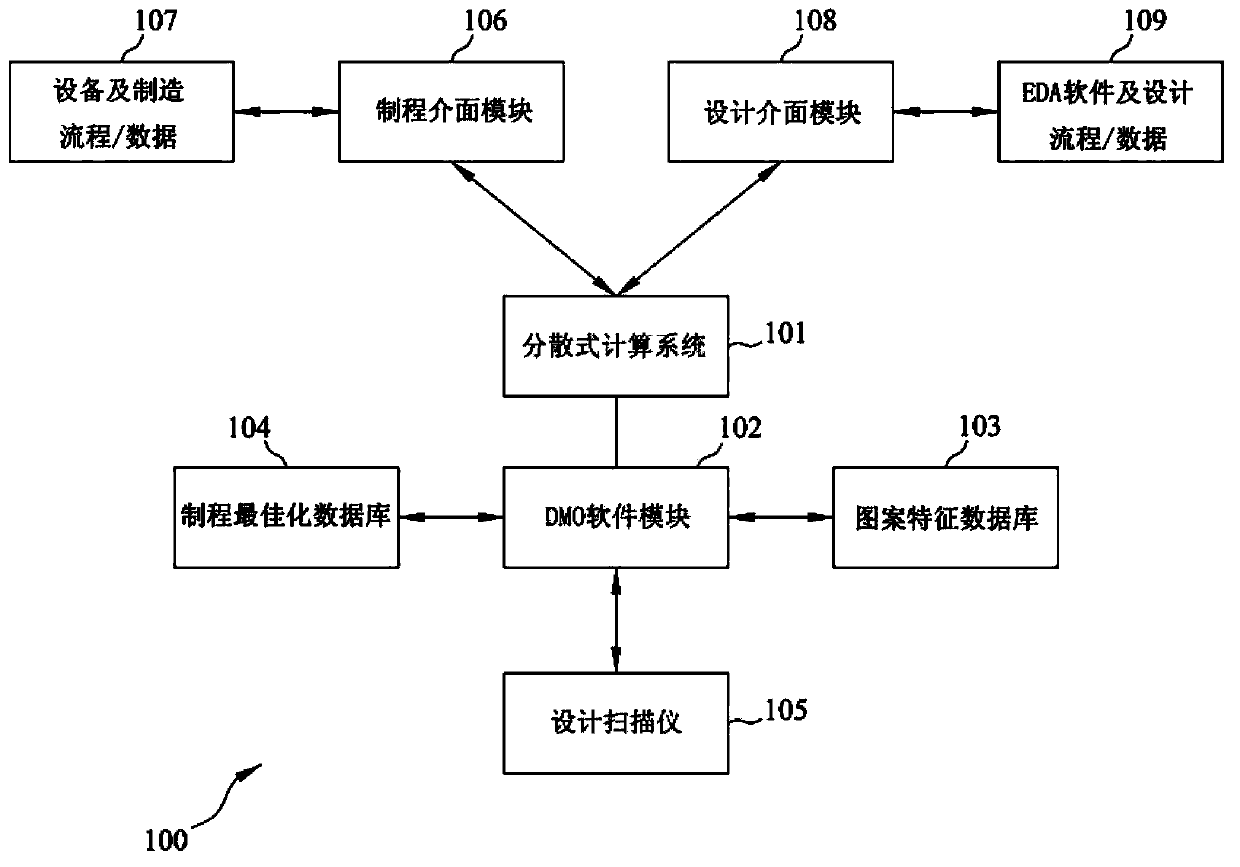
[0046] figure 1 It is a block diagram showing a design-based manufacturing optimization (DMO) apparatus 100 according to the present invention. The DMO device 100 includes a distributed computing system 101 and a DMO software module 102 , and further includes a pattern feature database 103 , a process optimization database 104 and a design scanner 105 . The distributed computing system 101 communicates with an EDA software and a design process 109 through a design interface module 108 , and communicates with equipment and a manufacturing process 107 through a manufacturing interface module 106 .

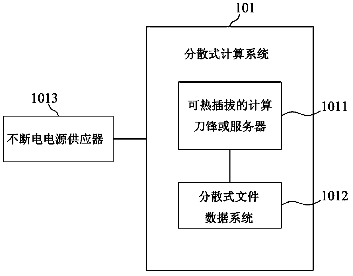
[0047] Such as figure 2 As shown, distributed computing system 101 is a fault-tolerant distributed computing system, which includes multiple redundant an...


PUM


Abstract

A design-based manufacturing optimization (DMO) server comprises a distributed computing system and a DMO software module incorporating with a design scanner to scan and analyze design data of a semiconductor device for optimizing manufacturing of the semiconductor device. The DMO software module sets up a pattern signature database and a manufacturing optimization database, generates design-based manufacturing recipes, interfaces with manufacturing equipment through a manufacturing interface module, and interfaces with electronic design automation suppliers for the design data through a design interface module. The DMO server executes the design-based manufacturing recipes for manufacturing optimization.

Description

technical field [0001] The present invention relates to semiconductor manufacturing process, in particular to a design-based device for optimizing semiconductor manufacturing process. Background technique [0002] The manufacture of semiconductors requires an advanced and cost-effective manufacturing environment. As semiconductor chips become smaller in size, their manufacturing costs also increase. In a modern fab, hundreds of machines are used to manufacture semiconductors, and the cost of each machine can range from tens of millions to hundreds of millions of dollars. [0003] The process of manufacturing integrated circuits often requires hundreds of sequential steps, each of which can result in a loss of yield. Therefore, in order to maintain the quality of its products in a semiconductor manufacturing plant, hundreds or thousands of process variables need to be tightly controlled. Among them, among several key capabilities currently under development, such as proces...

Claims


Application Information

Patent Timeline
Patent Type & Authority Applications(China)
IPC IPC(8): G06F17/50H01L21/67
CPCH01L22/12H01L22/20
Inventor 庄少特林志诚
Owner DMO SYST
Why Eureka
Try Eureka