Control circuit of power factor correcting circuit

A power factor correction and control circuit technology, applied in the direction of output power conversion devices, high-efficiency power electronic conversion, electrical components, etc., can solve the problems of power factor reduction, harmonic content increase, phase difference, etc., and achieve phase elimination poor effect

Active Publication Date: 2014-08-06
INVENTRONICS HANGZHOU
View PDF6 Cites 12 Cited by
  • Summary
  • Abstract
  • Description
  • Claims
  • Application Information

AI Technical Summary

Problems solved by technology

This will cause the input current Iin (of the AC input) and the input voltage Vin to have a phase difference in the entire circuit
This is because the input current Iin (of the AC input terminal) of the entire circuit is the sum of the current on the filter capacitor and the input current of the PFC circuit, and the phase of the current on the filter capacitor is 90 degrees ahead of the input voltage, that is, due to the filter capacitor Existence, the phase of the input current Iin is ahead of the phase of the input voltage Vin, so that the phase of the input current Iin and the phase of the input voltage Vin are inconsistent, resulting in a decrease in the power factor of the power supply and an increase in harmonic content

Method used


Image

  • Control circuit of power factor correcting circuit
  • Control circuit of power factor correcting circuit
  • Control circuit of power factor correcting circuit

Examples


Embodiment Construction

[0049] In order to make the above objects, features and advantages of the present invention more comprehensible, specific implementations of the present invention will be described in detail below in conjunction with the accompanying drawings.

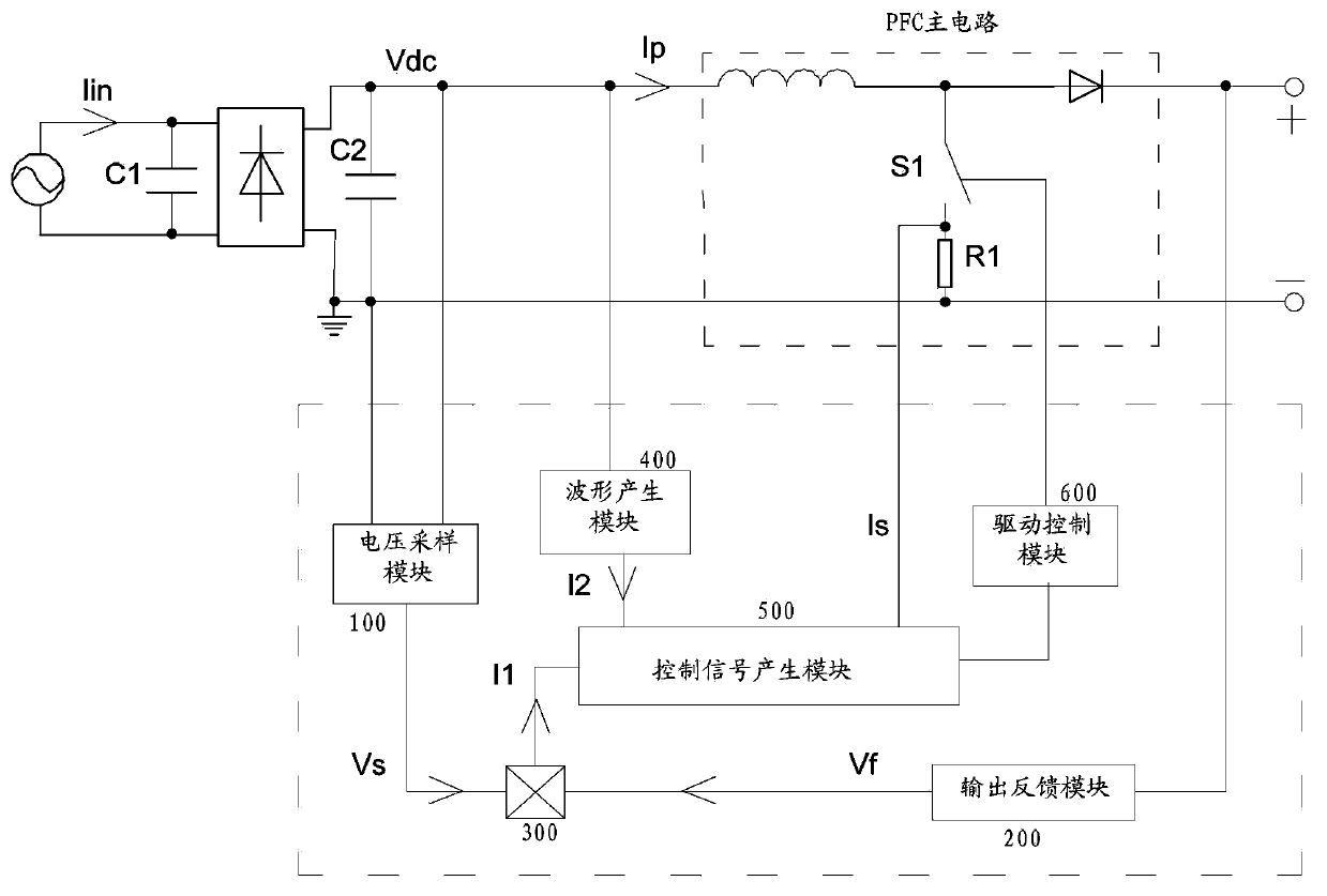
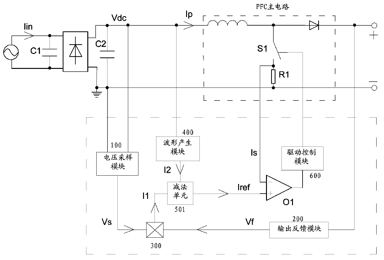
[0050] see figure 2 , which is a schematic diagram of Embodiment 1 of the control circuit in the power factor correction circuit provided by the present invention.

[0051] The control circuit in the power factor correction circuit provided in this embodiment includes: a voltage sampling module 100, an output feedback module 200, a multiplier 300, a waveform generation module 400, a control signal generation module 500 and a drive control module 600;

[0052] The voltage sampling module 100 is used for sampling the input voltage Vdc of the power factor correction circuit PFC, and outputting a voltage sampling signal Vs;

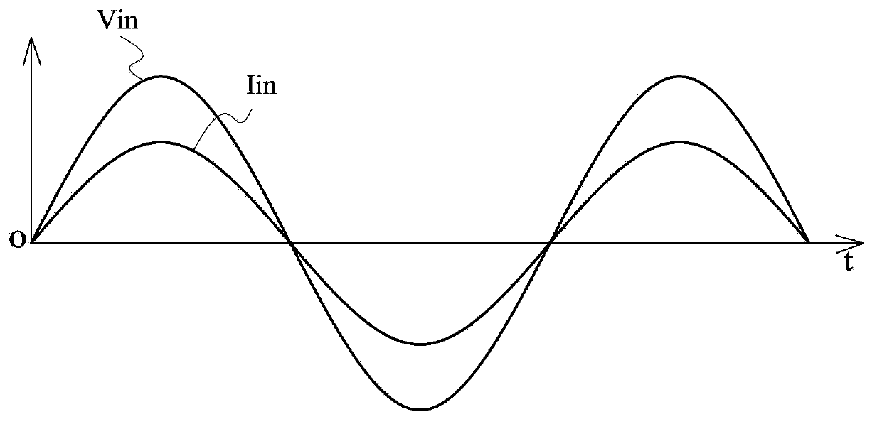
[0053] It should be noted that, the PFC circuit in this embodiment takes the Boost circuit as an example, as fig...


PUM


Abstract

A control circuit in a power factor correction (PFC) circuit comprises: a multiplier (300), used for multiplying a voltage sampling signal (Vs) by a feedback signal (Vf), and outputting a first signal (I1); and a waveform generating module (400), used for generating a second signal (I2) related to a filter capacitor (C1, C2) connected in parallel to an input end and / or an output end of a rectifier bridge. A control signal for controlling a state of a main switch transistor (S1) is generated by using the first signal, the second signal, and a current sampling signal (Is) of the main switch transistor in the PFC circuit. By controlling ON or OFF of the main switch transistor, a phase of a sum of an input current (Ip) and a total filter current (Ic) of the PFC circuit, that is, a phase of an input current (Iin) on an alternating current side, is same as a phase of an input voltage (Vin), thereby eliminating the difference between the phase of the input current and the phase of the input voltage occurring due to a phase difference caused by the filter capacitor.

Description

technical field [0001] The invention relates to the technical field of power factor correction, in particular to a control circuit in a power factor correction circuit. Background technique [0002] In a two-stage circuit or a single-stage power factor correction (PFC, Power Factor Correction) circuit, the output voltage of the sampling rectifier bridge is usually multiplied by the feedback signal at the output of the PFC, and the product is used as the reference signal of the switching tube current in the PFC. [0003] In this way, the input current of the PFC circuit can follow the change of the input voltage, so that the input current Iin (of the AC input terminal) in the entire circuit has the same phase as the input voltage Vin. Such as figure 1 As shown, the figure is a schematic diagram of the same phase of the input current Iin (of the AC input terminal) and the input voltage Vin in the prior art. [0004] However, in order to reduce high-frequency pollution to the...

Claims


Application Information

Patent Timeline
Patent Type & Authority Applications(China)
IPC IPC(8): H02M1/42
CPCH02M1/4225Y02B70/10Y02P80/10H02M1/4208
Inventor 姜德来葛良安吴莲
Owner INVENTRONICS HANGZHOU
Why Eureka
Try Eureka