Surrounding-gate-type nanowire transistor

A nanowire and transistor technology, applied in the field of gate-enclosed nanowire transistors, can solve the problems of low mobility of gate-enclosed nanowire transistors, and achieve the effect of increasing emission speed and mobility, and enhancing mobility

Active Publication Date: 2014-08-13
SHANGHAI HUALI MICROELECTRONICS CORP
View PDF6 Cites 4 Cited by
  • Summary
  • Abstract
  • Description
  • Claims
  • Application Information

AI Technical Summary

Problems solved by technology

[0005] The object of the present invention is to provide a gate-enclosed nanowire transistor to solve the problem that the mobility of the gate-enclosed nanowire transistor is too small

Method used


Image

  • Surrounding-gate-type nanowire transistor
  • Surrounding-gate-type nanowire transistor

Examples


Embodiment Construction

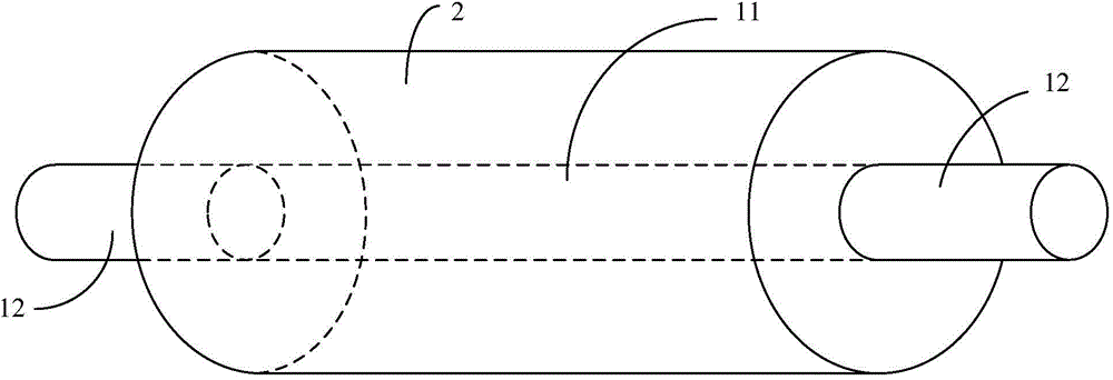
[0016] The gate-enclosed nanowire transistor of the present invention will be described in more detail below in conjunction with a schematic diagram, wherein a preferred embodiment of the present invention is shown, and it should be understood that those skilled in the art can modify the present invention described herein while still realizing the present invention. beneficial effect. Therefore, the following description should be understood as the broad knowledge of those skilled in the art, but not as a limitation of the present invention.

[0017] In the interest of clarity, not all features of an actual implementation are described. In the following description, well-known functions and constructions are not described in detail since they would obscure the invention with unnecessary detail. It should be appreciated that in the development of any actual embodiment, numerous implementation details must be worked out to achieve the developer's specific goals, such as changin...


PUM


Abstract

The invention discloses a surrounding-gate-type nanowire transistor. The transistor comprises a cylindrical main body structure, wherein the main body structure comprises a middle portion and two end portions located on the two sides of the middle portion, the middle portion is wrapped with grid electrodes in a surrounding mode and accordingly a surrounding gate is formed, the two end portions serve as a source electrode and a drain electrode respectively, the main body structure is mainly made of silicon and germanium, and the concentration of germanium in the middle portion is larger than the concentration of germanium on the two end portions. Due to the heterojunction structure of the source electrode, the drain electrode and channels, the valence band of the middle channel portion moves upwards, and accordingly the transmitting speed and the mobility ratio of a hole can be improved.

Description

technical field [0001] The invention relates to the technical field of semiconductors, in particular to a gate-surrounding nanowire transistor. Background technique [0002] Under the guidance of Moore's Law, the size of integrated circuit semiconductor devices is getting smaller and smaller, but it cannot be infinitely reduced. After shrinking to a certain extent, it will reach its physical limit, and severe short channel effect and gate leakage current will appear. This will be a challenge to the validity of Moore's Law. However, people are actively looking for alternative ways to shorten the device size to improve performance, so the industry focuses on the use of high-k materials and exploring new device structures, especially the latter. New device structures will be the direction and trend of future research and development of semiconductor devices. Silicon nanowire transistors are a novel device structure that is one of the most promising contenders for the 22nm te...

Claims


Application Information

Patent Timeline
Patent Type & Authority Applications(China)
IPC IPC(8): H01L29/78H01L29/06H01L29/12
CPCH01L29/125H01L29/36H01L29/775
Inventor 顾经纶
Owner SHANGHAI HUALI MICROELECTRONICS CORP
Why Eureka
Try Eureka