Method for carrying out insertion loss test through simple probe
A simple, impedance test strip technology, applied in the direction of measuring devices, measuring electrical variables, measuring resistance/reactance/impedance, etc., can solve the problems of expensive probe station, difficult operation, easy damage, etc., and achieve easy promotion, accurate results, good stability effect
- Summary
- Abstract
- Description
- Claims
- Application Information
AI Technical Summary
Problems solved by technology
Method used
Image

Examples
Embodiment
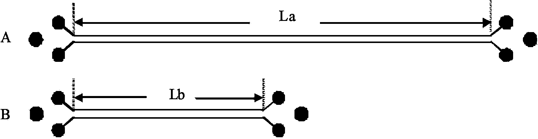
[0027] As attached figure 1 As shown, design two traces on the circuit board. Trace A is longer than trace B. Trace B should not be too short. The difference between the length of trace A and B should be more than 4 inches. Then, in this example, A, B The lengths of the two traces are La and Lb respectively.
[0028] Using a 12-port vector network analyzer VNA combined with a self-made simple probe to measure the insertion loss of the two signal traces A and B and the vias, respectively, ILA and ILB.
[0029] After the measurement, the insertion loss per unit length is calculated according to the formula: (ILA-ILB) / (La-Lb).
[0030] At this time, the calculated insertion loss value is the insertion loss of the PCB trace in the true sense, and is not affected by the probe and the via.
[0031] In the PCB routing design, ensure that the stack, test points and vias of the two signal lines are exactly the same. Avoid affecting the test results due to other reasons.
PUM
 Abstract
Description
Claims
Application Information
 - Generate Ideas
- Intellectual Property
- Life Sciences
- Materials
- Tech Scout
- Unparalleled Data Quality
- Higher Quality Content
- 60% Fewer Hallucinations
Browse by: Latest US Patents, China's latest patents, Technical Efficacy Thesaurus, Application Domain, Technology Topic, Popular Technical Reports.
© 2025 PatSnap. All rights reserved.Legal|Privacy policy|Modern Slavery Act Transparency Statement|Sitemap|About US| Contact US: help@patsnap.com