Image sensor glass cavity wall manufacturing method
A technology of image sensor and manufacturing method, which is applied in semiconductor/solid-state device manufacturing, electric solid-state devices, semiconductor devices, etc., can solve the problems of high manufacturing cost and low yield rate, and achieve the effect of avoiding photoresist forming and bonding process
- Summary
- Abstract
- Description
- Claims
- Application Information
AI Technical Summary
Problems solved by technology
Method used
Image


Examples
Embodiment 1
[0024] Embodiment 1: A method for manufacturing an image sensor glass chamber wall, comprising the following steps:
[0025] (1) Make an ultra-thin square glass tube, such as figure 1 As shown, the wall thickness of the square glass tube is 50 μm, and the cross-sectional size of the square glass tube matches the size of the pattern on the image sensor wafer;
[0026] (2) Cut the glass tube into a single square piece with a diamond wire, a diamond blade or a laser, and the thickness of the square piece is 50 μm;
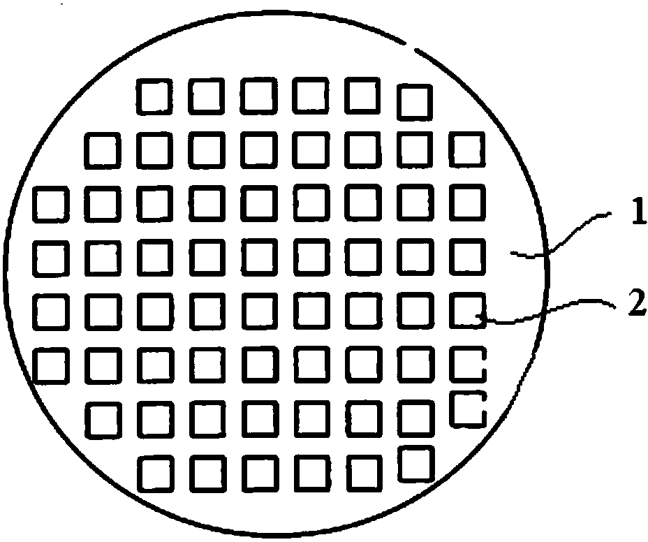
[0027] (3) if figure 2 As shown, one surface of several square sheets 2 is dipped in adhesive 4, and pressed onto the glass substrate 1 to form several square cavities corresponding to the patterns on the image sensor wafer one by one. The thickness is 100 μm; the curing process is carried out after pressing, the temperature of the curing process is 50 ° C, and the time is 30 min;
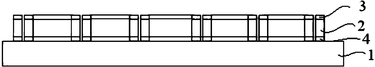
[0028] (4) if image 3 As shown, the adhesive 3 is coated on the other surface of...
Embodiment 2
[0030] Embodiment 2: A method for manufacturing an image sensor glass chamber wall, comprising the following steps:
[0031] (1) Make an ultra-thin square glass tube, such as figure 1 As shown, the wall thickness of the square glass tube is 300 μm, and the cross-sectional size of the square glass tube matches the size of the pattern on the image sensor wafer;
[0032] (2) Cut the glass tube into a single square piece with a diamond wire, a diamond blade or a laser, and the thickness of the square piece is 200 μm;
[0033] (3) if figure 2 As shown, one surface of several square sheets 2 is coated with adhesive 4, and pressed onto the glass substrate 1 to form several square cavities corresponding to the patterns on the image sensor wafer one by one, and the glass substrate The thickness is 500μm; the curing process is carried out after pressing, the temperature of the curing process is 150 ° C, and the time is 10 min;
[0034] (4) if image 3 As shown, the adhesive 3 is co...
Embodiment 3
[0036] Embodiment 3: A method for manufacturing an image sensor glass chamber wall, comprising the following steps:
[0037] (1) Make an ultra-thin square glass tube, such as figure 1 As shown, the wall thickness of the square glass tube is 100 μm, and the cross-sectional size of the square glass tube matches the size of the pattern on the image sensor wafer;
[0038] (2) Cut the glass tube into a single square piece with a diamond wire, a diamond blade or a laser, and the thickness of the square piece is 100 μm;
[0039] (3) if figure 2 As shown, the adhesive 4 is coated on the surface of the glass substrate, and the position of the adhesive coating area corresponds to the pressing area of the square sheet on the glass substrate, and the shape and size of the adhesive coating area are similar to those of the square sheet. The shape and size of the glass substrate are consistent; then the square sheet is pressed onto the glass substrate 1 to form a number of square caviti...
PUM
 Abstract
Description
Claims
Application Information
 - Generate Ideas
- Intellectual Property
- Life Sciences
- Materials
- Tech Scout
- Unparalleled Data Quality
- Higher Quality Content
- 60% Fewer Hallucinations
Browse by: Latest US Patents, China's latest patents, Technical Efficacy Thesaurus, Application Domain, Technology Topic, Popular Technical Reports.
© 2025 PatSnap. All rights reserved.Legal|Privacy policy|Modern Slavery Act Transparency Statement|Sitemap|About US| Contact US: help@patsnap.com