Supercharge Your Innovation With Domain-Expert AI Agents!

Laminated packaging body based on glass adapter plate and preparation method of laminated packaging body

A technology of glass interposer and laminated packaging, which is applied in semiconductor/solid-state device manufacturing, electrical solid-state devices, semiconductor devices, etc., and can solve problems such as incomplete welding, electrical performance problems, and hidden cracks in welding areas.

Active Publication Date: 2015-03-11
NAT CENT FOR ADVANCED PACKAGING
View PDF6 Cites 2 Cited by
  • Summary
  • Abstract
  • Description
  • Claims
  • Application Information

AI Technical Summary

Problems solved by technology

However, this technology faces a problem at the same time that the interconnection between chips is realized through repeated production of leads. This technology will cause a series of electrical performance problems and reliability problems, such as incomplete welding and cracks in the welding area. question

Method used


Image

  • Laminated packaging body based on glass adapter plate and preparation method of laminated packaging body
  • Laminated packaging body based on glass adapter plate and preparation method of laminated packaging body
  • Laminated packaging body based on glass adapter plate and preparation method of laminated packaging body

Examples


Embodiment Construction

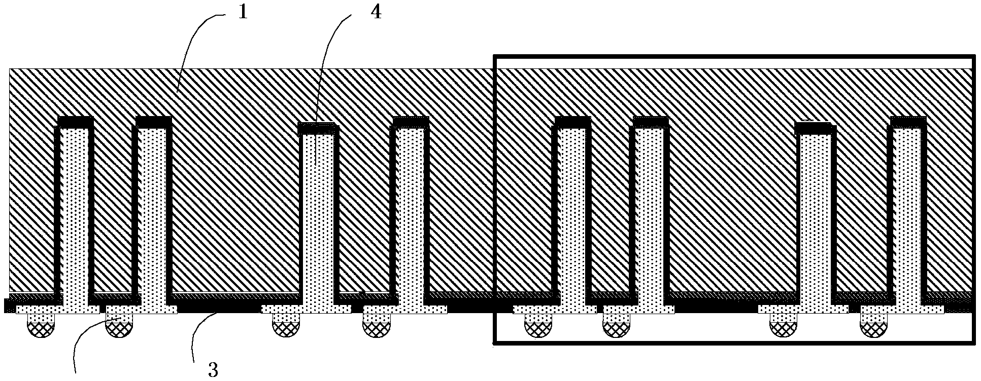
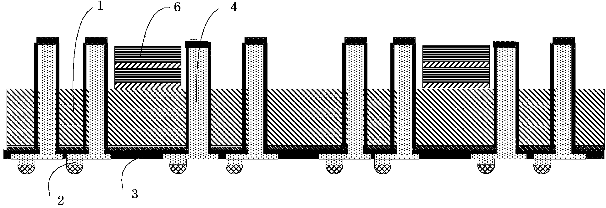
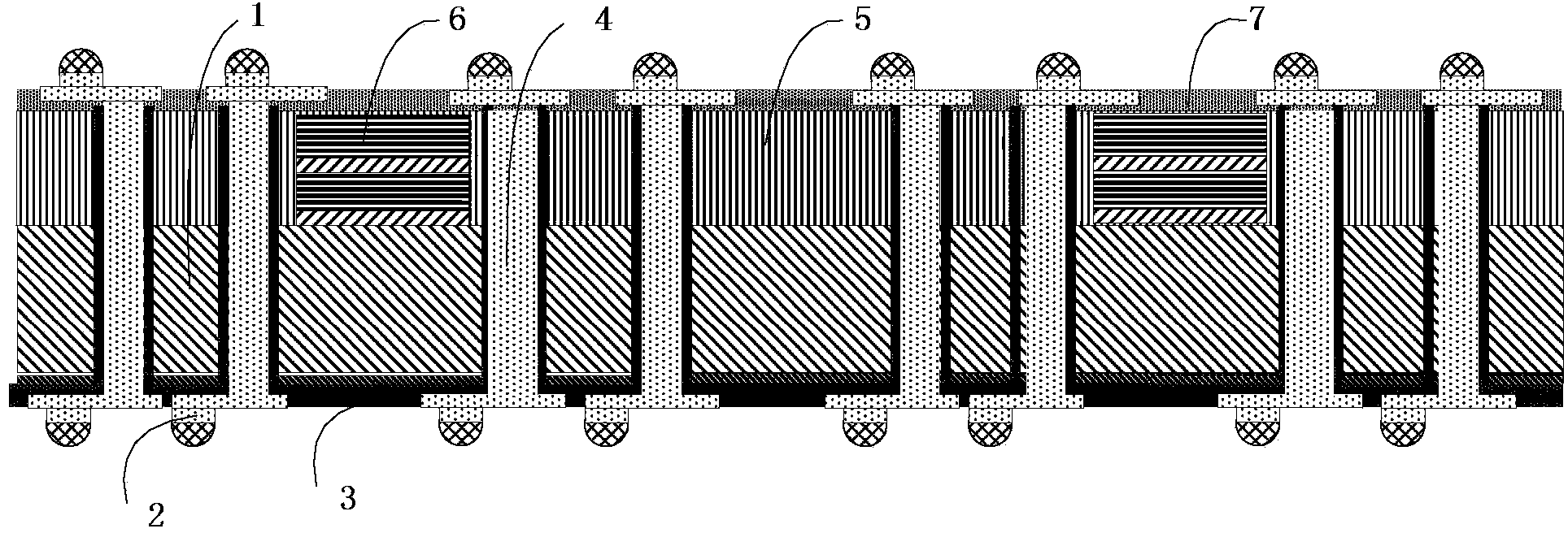
[0023] The first step of the method for preparing a laminated package based on the glass interposer provided by the present invention is to provide a glass interposer 1 . Vias are then made on it, using techniques such as wet etching, dry etching, deep reactive ion etching, or laser etching. Vias can have an aspect ratio of 10:1, a depth ranging from 30 to 300 microns, and a diameter as small as 5 microns. Subsequently, the filling of the metal in the through hole is completed to form the metal pillar 4. The filling method can be conventional electroplating filling or chemical vapor deposition, preferably electroplating filling. The filled metal material can be copper or tungsten, preferably copper. If the hole depth value is small. And prepare the front wiring 2 and the insulating layer 3, the schematic diagram of the structure after the end is as follows figure 1 As shown, the black box represents the area of ​​a chip.

[0024] Next, the back side of the glass interposer...


PUM


Abstract

The invention discloses a laminated packaging body based on a glass adapter plate and a preparation method of the laminated packaging body. Chip layers are stacked on the upper surface of the glass adapter plate subjected to back thinning and head exposure; the exterior and interlayer of the chip layers are filled with sealing materials; passivation layers are arranged on the upper surfaces of the sealing materials and the chip layers; front wiring is embedded in the front passivation layer of the glass adapter plate; back wiring is embedded in the back passivation layer; and the back wiring and the front wiring are connected with each other through metal posts penetrating through the glass adapter plate and a package. According to the laminated packaging body disclosed by the invention, direct interconnection of the stacked chips from the upper surface to the lower surface of the glass adapter plate is realized, and laminated packaging based on the glass adapter plate is realized. The problems of a traditional method that when electric connection between the upper surface and the lower surface is achieved by using a multilayer complex wiring process, the manufacturing cost is high and the yield is low are solved.

Description

technical field [0001] The invention discloses a laminated packaging body based on a glass transfer plate, and the invention relates to the field of semiconductor packaging. Background technique [0002] With the development of people's requirements for electronic products in the direction of miniaturization, multi-function, and environmental protection, people strive to make electronic systems smaller and smaller, with higher integration and more functions. , resulting in many new technologies, new materials and new designs, among which stacked chip packaging technology and system-in-package (System-in-Package, SIP) technology are typical representatives of these technologies. [0003] Wafer-level packaging takes the wafer as the processing object. Multiple chips are packaged and tested on the wafer at the same time. Finally, they are cut into individual devices and assembled by reverse welding. It reduces the package size to the chip size. An advanced ultra-small packagin...

Claims


Application Information

Patent Timeline
IPC IPC(8): H01L23/12H01L21/58
CPCH01L2224/04105H01L2224/12105H01L2224/18H01L2224/32225H01L2224/73267H01L2224/92244
Inventor 王谆姜峰张文奇
Owner NAT CENT FOR ADVANCED PACKAGING
Features
  • R&D
  • Intellectual Property
  • Life Sciences
  • Materials
  • Tech Scout
  • Unparalleled Data Quality
  • Higher Quality Content
  • 60% Fewer Hallucinations
Learn More