Apparatus for single wafer etching

A technology for etching equipment and wafers, used in electrical components, semiconductor/solid-state device manufacturing, circuits, etc., can solve problems such as deteriorating wafer flatness, and achieve the effect of improving flatness

Active Publication Date: 2014-08-20
LG SILTRON
View PDF5 Cites 5 Cited by
  • Summary
  • Abstract
  • Description
  • Claims
  • Application Information

AI Technical Summary

Problems solved by technology

However, for a typical single-wafer etching apparatus, the etching solvent supplied at the center of the wafer moves toward the circumferential direction of the wafer due to centrifugal force, and as the reaction between the etching solvent and the surface of the wafer is Repeat, etching is more severe towards the circumference of the wafer depending on the temperature of the etch solvent, which in turn can degrade the flatness of the wafer

Method used


Image

  • Apparatus for single wafer etching
  • Apparatus for single wafer etching
  • Apparatus for single wafer etching

Examples


Embodiment Construction

[0031] Hereinafter, the embodiments will be described in detail with reference to the accompanying drawings. However, the present invention can be implemented in many different ways and should not be construed as limited to the embodiments set forth herein; additions, modifications and changes can easily be included in another modified invention or fall within the spirit of the present disclosure. and alternative embodiments within the scope.

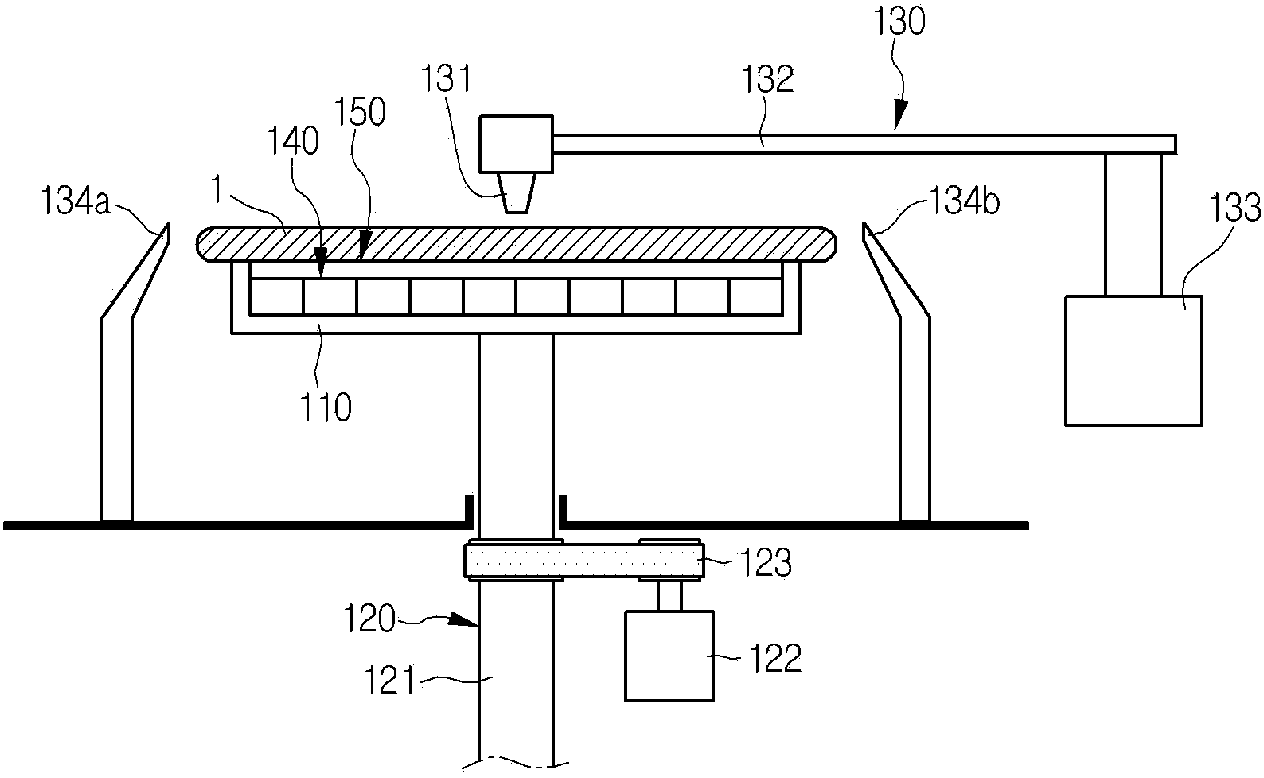
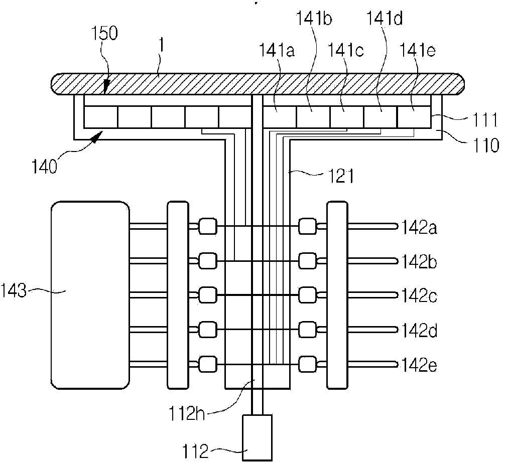
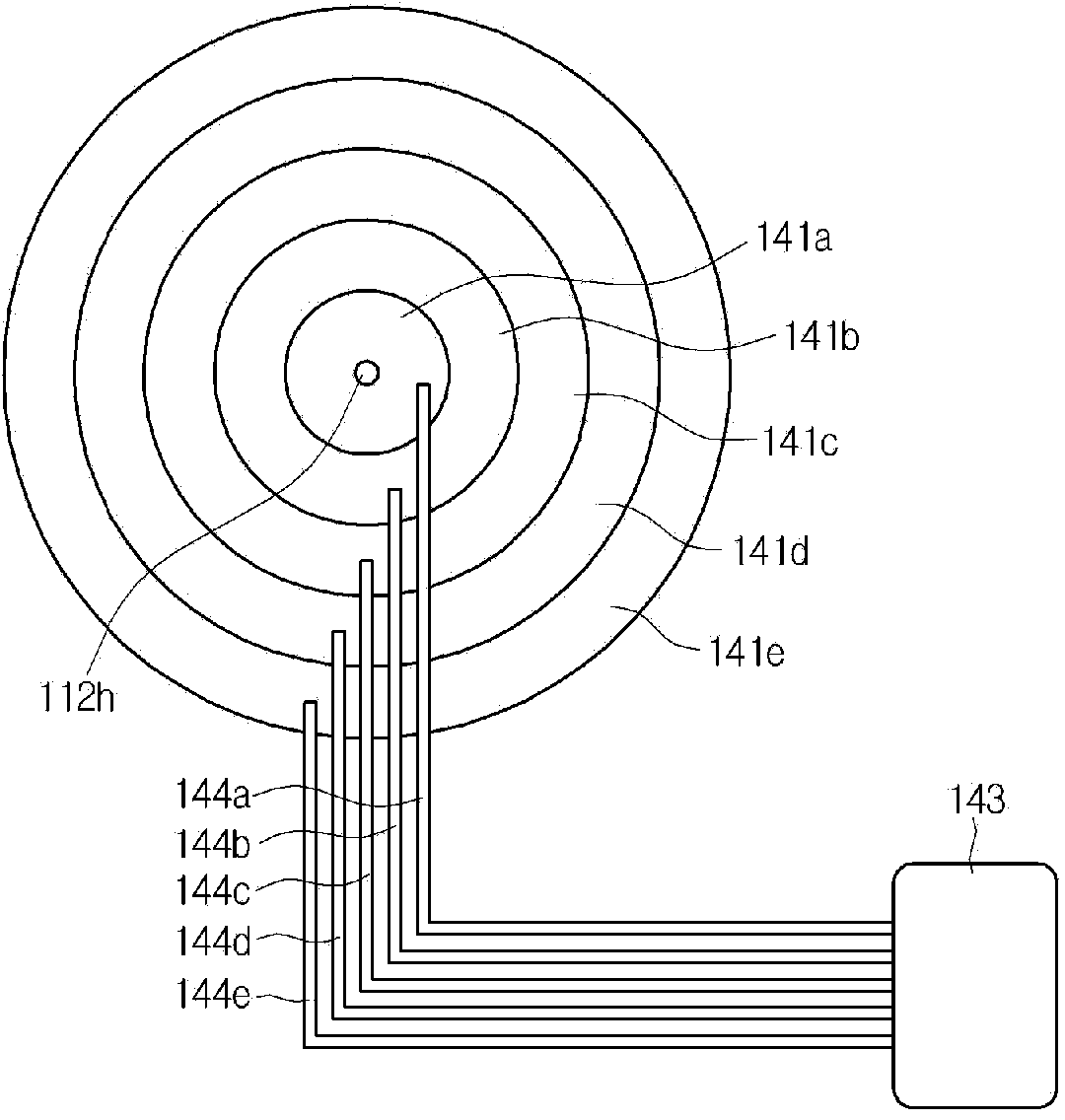
[0032] figure 1 and figure 2 shows a first embodiment of a single wafer etching apparatus according to the present invention, and image 3 One example of the heating device of the single-wafer etching apparatus according to the present invention is shown.

[0033] Such as figure 1 and figure 2 As shown, an example of the single-wafer etching equipment according to the present invention may include a turntable 110 on which a wafer 1 is installed, a driving device 120 for rotating the turntable 110, and an etching solvent sprayed o...


PUM


Abstract

Provided is a single wafer etching apparatus etching wafers one at a time. According to the present invention, the single wafer etching apparatus may not only discharge gas by vibrating the wafer even in the case that gas, a byproduct of an etching reaction, is generated, but may also prevent the gas from adsorbing on a surface of the wafer. Also, since the single wafer etching apparatus may directly heat each region of the wafer, the single wafer etching apparatus may uniformly maintain a reaction temperature by heating to higher temperatures from a circumferential direction toward the center of the wafer, even in the case that the temperature of an etching solution increases from the center of the wafer toward the circumferential direction due to the fact that etching is performed while the etching solution moves from the center of the wafer toward the circumferential direction. Therefore, the single wafer etching apparatus may not only uniformly maintain a degree of etching regardless of a position on the wafer, but may also increase flatness.

Description

technical field [0001] The present disclosure relates to a single wafer etching apparatus in which wafers rotated by a turntable are etched one at a time by an etching solvent sprayed through nozzles. Background technique [0002] Etching is generally performed to eliminate damages generated during machining of the wafer. [0003] Recently, there has been a tendency in the semiconductor industry to increase the diameter of wafers and to increase the integration density and pattern fineness of semiconductor devices. Batch type etching equipment not only increases in size to etch large diameter wafers, but also increases consumption of etching solvents. Therefore, single-wafer etching apparatuses that process one wafer at a time have been widely used in order to efficiently etch large-diameter wafers. [0004] Typical single-wafer etching equipment is disclosed in Korean Patent Applications 2008-0019366, 2008-7019037, and 2009-0002214, in which the wafer is fixed on the turn...

Claims


Application Information

Patent Timeline
Patent Type & Authority Applications(China)
IPC IPC(8): H01L21/306
CPCH01L21/67109H01L21/6708H01L21/306
Inventor 李在桓崔恩硕
Owner LG SILTRON
Why Eureka
Try Eureka