Package for housing electronic components, and electronic device

A technology of electronic components and packages, which is applied in the direction of circuit devices, printed circuit components, printed circuits connected with non-printed electrical components, etc., and can solve problems such as signal phase difference

Active Publication Date: 2014-08-20
KYOCERA CORP
View PDF3 Cites 6 Cited by
  • Summary
  • Abstract
  • Description
  • Claims
  • Application Information

AI Technical Summary

Problems solved by technology

Also, due to the difference in the length of the signal lines, there will be a phase difference in the signal transmitted in each signal line

Method used


Image

  • Package for housing electronic components, and electronic device
  • Package for housing electronic components, and electronic device
  • Package for housing electronic components, and electronic device

Examples


Embodiment Construction

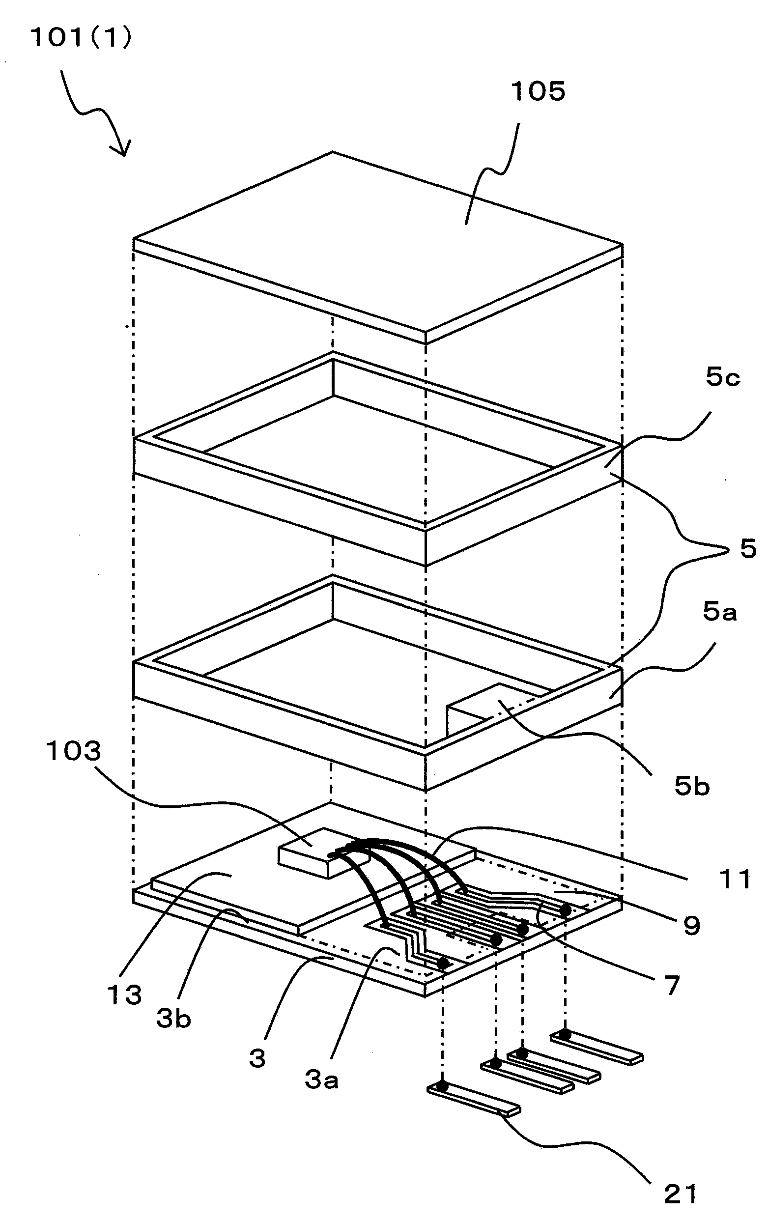
[0026] Hereinafter, the electronic component housing package 1 (it will only be called a package 1 hereafter) and the electronic device 101 provided with it in each embodiment of this invention are demonstrated in detail using drawings. However, each drawing referred to below is a structure shown more simplified than actual in order to explain this invention. Therefore, the package and the electronic device according to the present invention can include arbitrary components not shown in the drawings referred to in this specification. In addition, the scale of each figure differs from an actual one.

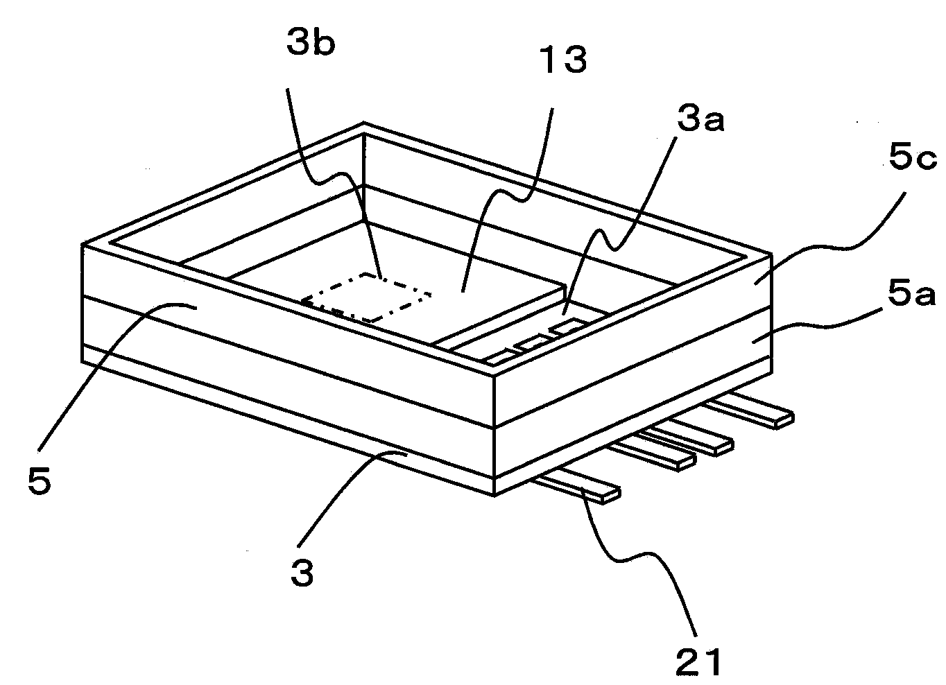
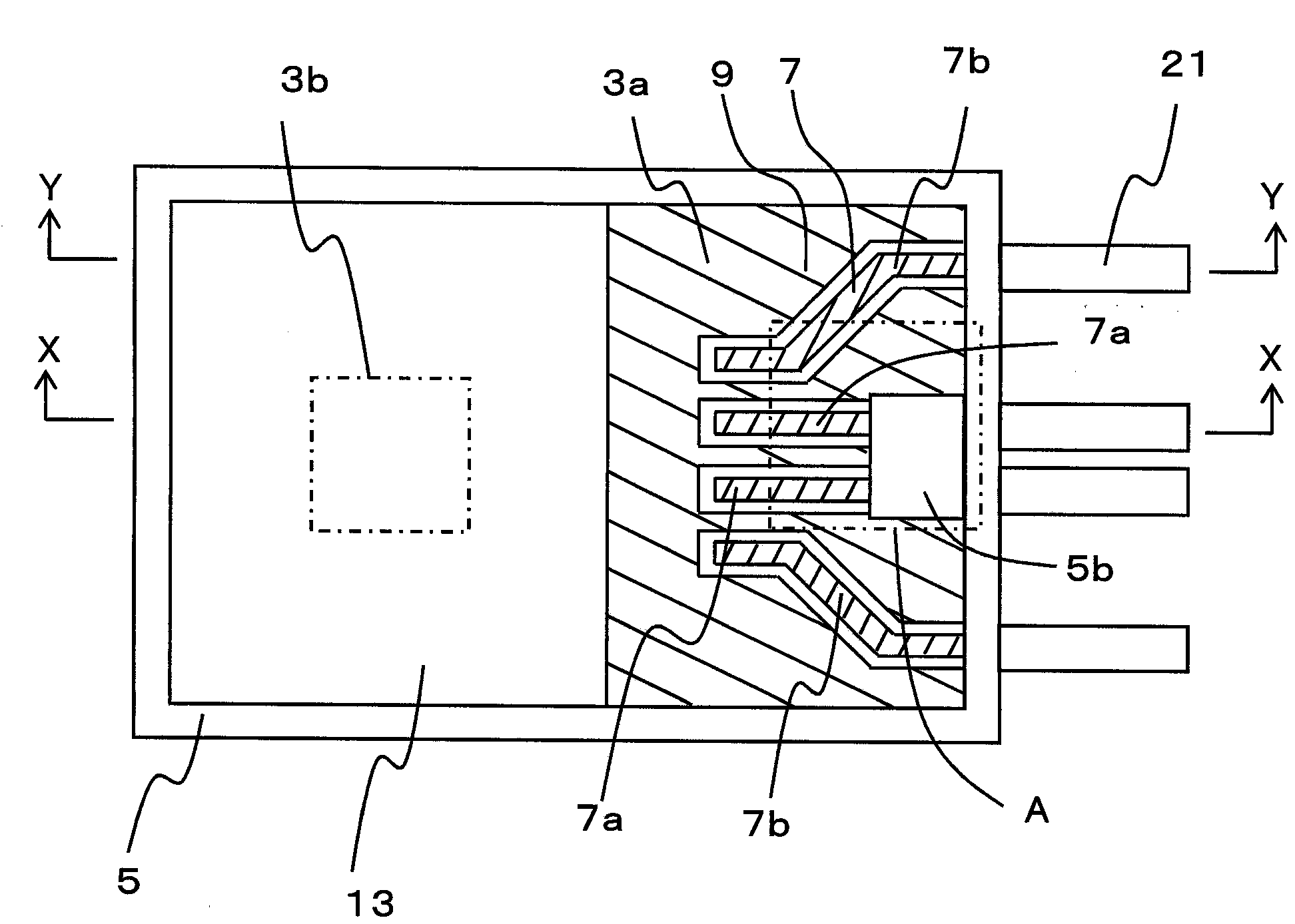
[0027] exist Figure 1 ~ Figure 5B The package of the first embodiment is shown. The package 1 of the first embodiment includes a container main body composed of a substrate 3 and a frame 5 . The substrate 3 has a dielectric region 3a made of a dielectric, and a mounting region 3b for electronic components adjacent thereto. In the mounting area 3b, the electronic component 103...


PUM


Abstract

While it is necessary for a package for housing electronic components to be furnished with numerous wire conductors, phase differences of signals, caused by differences in the signal transmission distance among wire conductors, is a problem. This package for housing electronic components has: a substrate having a dielectric area and an electronic component mounting area; a frame furnished to enclose the dielectric area and the mounting area; and a plurality of wire conductors arranged in the dielectric area of the substrate. The plurality of wire conductors have first wire conductors arranged in the dielectric area from directly below the frame, and second wire conductors of longer signal transmission distance than the first wire conductors. The frame, which comprises a dielectric, is provided with a protruding part protruding from the inside peripheral surface, and covering the first wire conductors at least in part.

Description

technical field [0001] The present invention relates to an electronic component housing package and an electronic device that accommodate electronic components such as semiconductor elements. Such electronic devices are used in various electronic equipment. Background technique [0002] As an electronic component housing package (hereinafter also simply referred to as a package) that accommodates an electronic component, there is, for example, a package in which a plurality of signal lines are radially formed on the upper surface of a dielectric substrate. The signal line is connected to the electronic component mounted on the dielectric substrate via a plurality of pads. [0003] Prior art literature [0004] patent documents [0005] Patent Document 1: JP Unexamined Patent Publication No. 9-275145 [0006] Summary of the invention [0007] The problem to be solved by the invention [0008] However, since the plurality of signal lines are arranged radially, the length...

Claims


Application Information

Patent Timeline
Patent Type & Authority Applications(China)
IPC IPC(8): H01L23/04
CPCH01L2224/48091H01L23/49861H05K1/18H01L23/057H01L2924/3011H05K1/0213H05K1/024H05K2201/09336H01L2924/00014H01L2924/00
Inventor 辻野真广川头芳规
Owner KYOCERA CORP
Why Eureka
Try Eureka