Structure and manufacturing method of optical transceiver module

An optical transceiver module and spacer technology, which is applied in the coupling of optical waveguides, electrical components, and electrical solid-state devices, etc., can solve the problems of unbalanced technology maturity, technical difficulties in optoelectronic parts, and high access thresholds, and achieve convenient splicing. Simple, low cost, thinning effect

Active Publication Date: 2014-08-27
NAT CENT FOR ADVANCED PACKAGING
View PDF8 Cites 11 Cited by
  • Summary
  • Abstract
  • Description
  • Claims
  • Application Information

AI Technical Summary

Problems solved by technology

[0006] In addition, optical transceiver modules and components can be divided into pure electrical parts and optoelectronic parts. Due to the unbalanced technology maturity, the technical difficulties of the optoelectronic part are relatively high, and the entry threshold is relatively high. Field Constraints

Method used


Image

  • Structure and manufacturing method of optical transceiver module
  • Structure and manufacturing method of optical transceiver module
  • Structure and manufacturing method of optical transceiver module

Examples


Embodiment Construction

[0043] The present invention will be further described below in conjunction with specific drawings and embodiments.

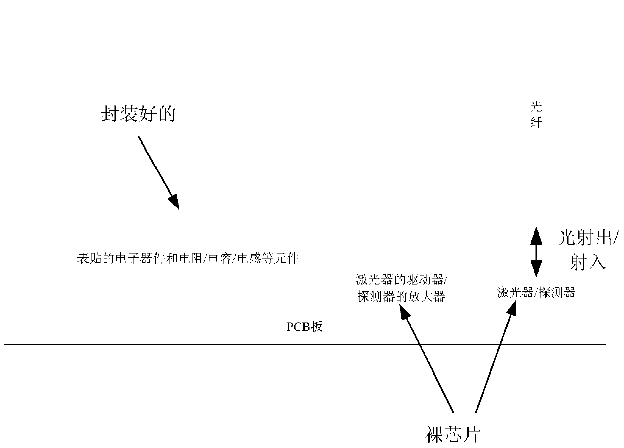
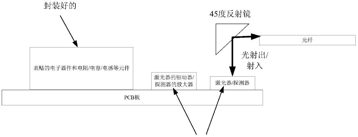
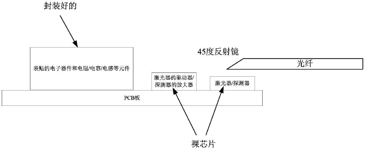
[0044] The structure of the optical transceiver module proposed by the present invention, such as Figure 5As shown, a spacer 11 is included, and a pure electric part 101 and a photoelectric part 201 that are independent and electrically connected are adjacently carried on the spacer 11 .

[0045] The optoelectronic part 201 includes a carrier 1, the side of the carrier 1 is mounted on the spacer 11, one side of the carrier 1 is fixed to the spacer 11, the other side and the top surface are provided with metal wiring 2, and the top surface of the carrier 1 The metal wiring 2 is provided with bumps 3, and the photoelectric conversion chip 4 is mounted upside down on the top surface of the carrier 1 through the bumps 3, and is electrically connected with the metal wiring 2; Holes 12, one or more optical fibers 7 are inserted laterally in each through hole 12 of ...


PUM


Abstract

The invention provides a structure of an optical transceiver module. The structure comprises a cushion block, wherein a pure electricity portion and a photoelectricity portion are borne by the cushion block in a neighboring mode, the pure electricity portion and the photoelectricity portion are independent from each other and electrically connected with each other, the photoelectricity portion comprises a carrier piece, the carrier piece is installed on the cushion block in a sidewise mode, metal wires are arranged on the other side and the top surface of the cushion block, a photovoltaic conversion chip is installed on the top surface of the carrier piece with the bottom upward and electrically connected with the metal wires, one or more transverse through holes are formed in the carrier piece, one or more optical fibers are transversely inserted into the through holes of the carrier piece respectively, the photovoltaic conversion chip is provided with one ore more working units, and the active areas of the working units on the front side of the photovoltaic conversion chip are aligned with the optical fibers in the through holes one to one. The pure electricity portion comprises a base plate installed on the cushion block, and an electric chip is installed on the portion, close to the photoelectricity portion, of the edge of the pure electricity portion, and connected with the metal wire on the side face of the carrier piece through a metal bonding wire. According to the structure of the optical transceiver module, the purpose that in the optical transceiver module, the direction of the optical fibers is parallel to the plane of a circuit board is achieved.

Description

technical field [0001] The invention relates to a photoelectric device, in particular to an optical transceiver module. Background technique [0002] Although the vertical cavity surface emitting laser (VCSEL) and the surface receiving detector are directly coupled face-to-face with the fiber, although the coupling efficiency is high, the direction of the fiber is perpendicular to the vertical cavity surface emitting laser (VCSEL) and the surface receiving detector; usually, the vertical cavity surface emitting laser ( VCSEL) and the upper and lower surfaces of the surface photodetector are parallel to the plane of the circuit board, so the direction of the optical fiber and the plane of the circuit board are perpendicular to each other at this time; due to the limited bending radius of the optical fiber, especially the large bending radius of the optical fiber ribbon, so The application scenario of this coupling method requires a larger space in the vertical direction of th...

Claims


Application Information

Patent Timeline
Patent Type & Authority Applications(China)
IPC IPC(8): G02B6/42
CPCH01L2224/48091
Inventor 李宝霞
Owner NAT CENT FOR ADVANCED PACKAGING
Why Eureka
Try Eureka