
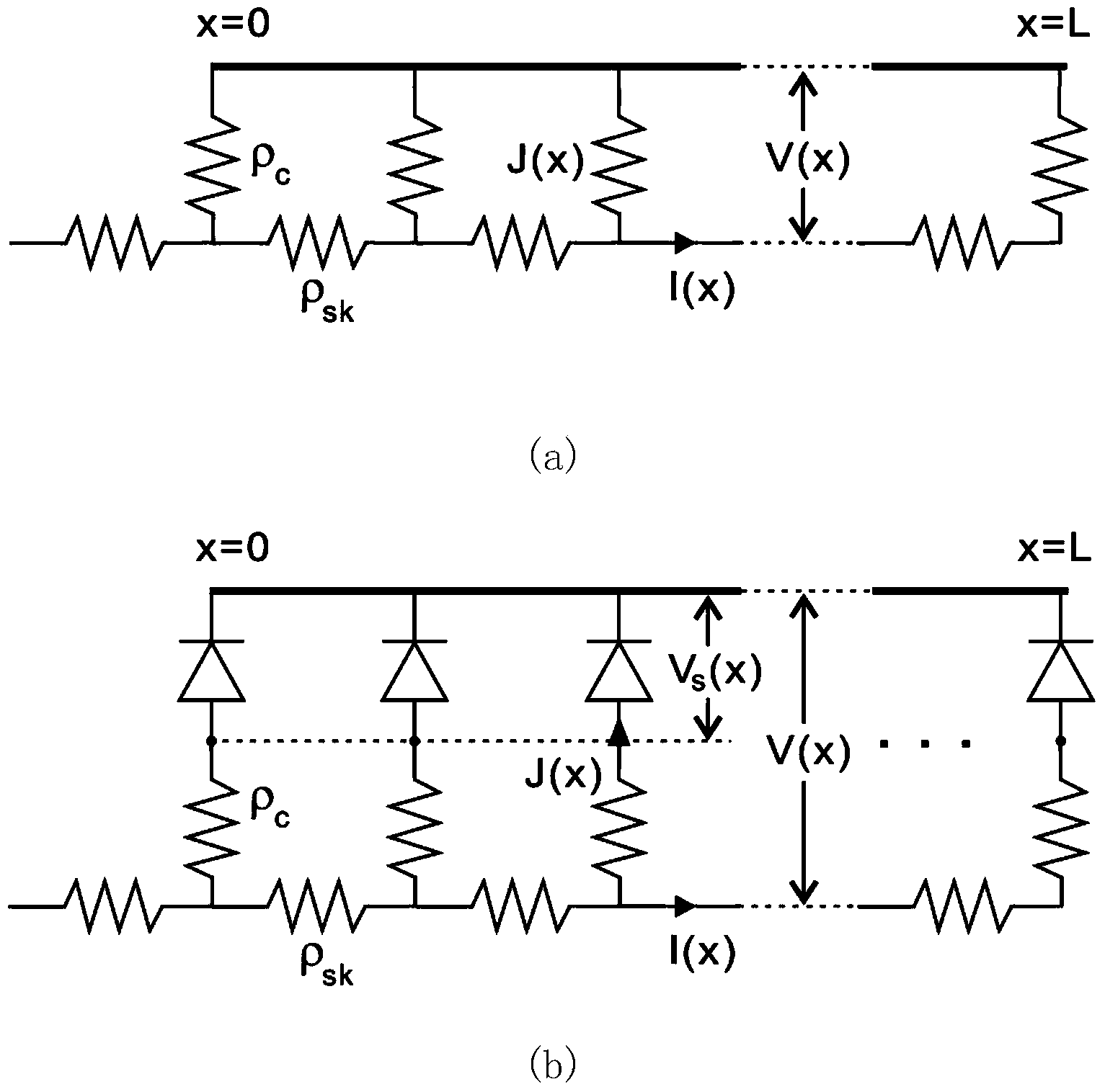
Metal-semiconductor contact nonlinear transmission line model and parameter fitting method

A nonlinear transmission line, metal-semiconductor technology, applied in the field of detection and characterization of the structural performance of semiconductor devices, can solve problems such as inaccurate description of nonlinear metal-semiconductor electrical properties

Inactive Publication Date: 2014-09-10
SHANGHAI INST OF TECHNICAL PHYSICS - CHINESE ACAD OF SCI
View PDF4 Cites 13 Cited by
  • Summary
  • Abstract
  • Description
  • Claims
  • Application Information

AI Technical Summary

Problems solved by technology

A single contact resistance can no longer accurately describe the electrical characteristics of nonlinear metal-semiconductor contacts

Method used


Image

  • Metal-semiconductor contact nonlinear transmission line model and parameter fitting method
  • Metal-semiconductor contact nonlinear transmission line model and parameter fitting method
  • Metal-semiconductor contact nonlinear transmission line model and parameter fitting method

Examples


Embodiment Construction

[0035] Based on the above methods, the present invention will be further described in detail below through the embodiments and accompanying drawings.

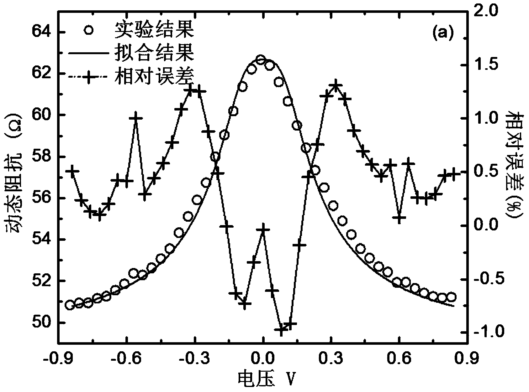
[0036] The metal-semiconductor system to be detected is metal tin Sn in contact with p-type mercury cadmium telluride HgCdTe (cadmium component is 0.303), and the carrier concentration is 4.48×10 15 cm -3 , the semiconductor film resistivity ρ s -1.55×10 3 Ω / □. Richardson's constant A* of hole = 66A / (cm K) 2 . Barrier height φ, ideality factor n, specific contact resistance ρ in nonlinear transmission line model c and the sheet resistivity ρ of the semiconductor material under the electrode sk as the physical parameters to be fitted.

[0037] The dimensions of the two metal electrodes to be tested are length L=20 μm, width w=1000 μm, and the distance between the electrodes is 15 μm. The resistance of the semiconductor material connected in series between the electrodes can be calculated as 23.3Ω from the sheet resistivit...


PUM


Abstract

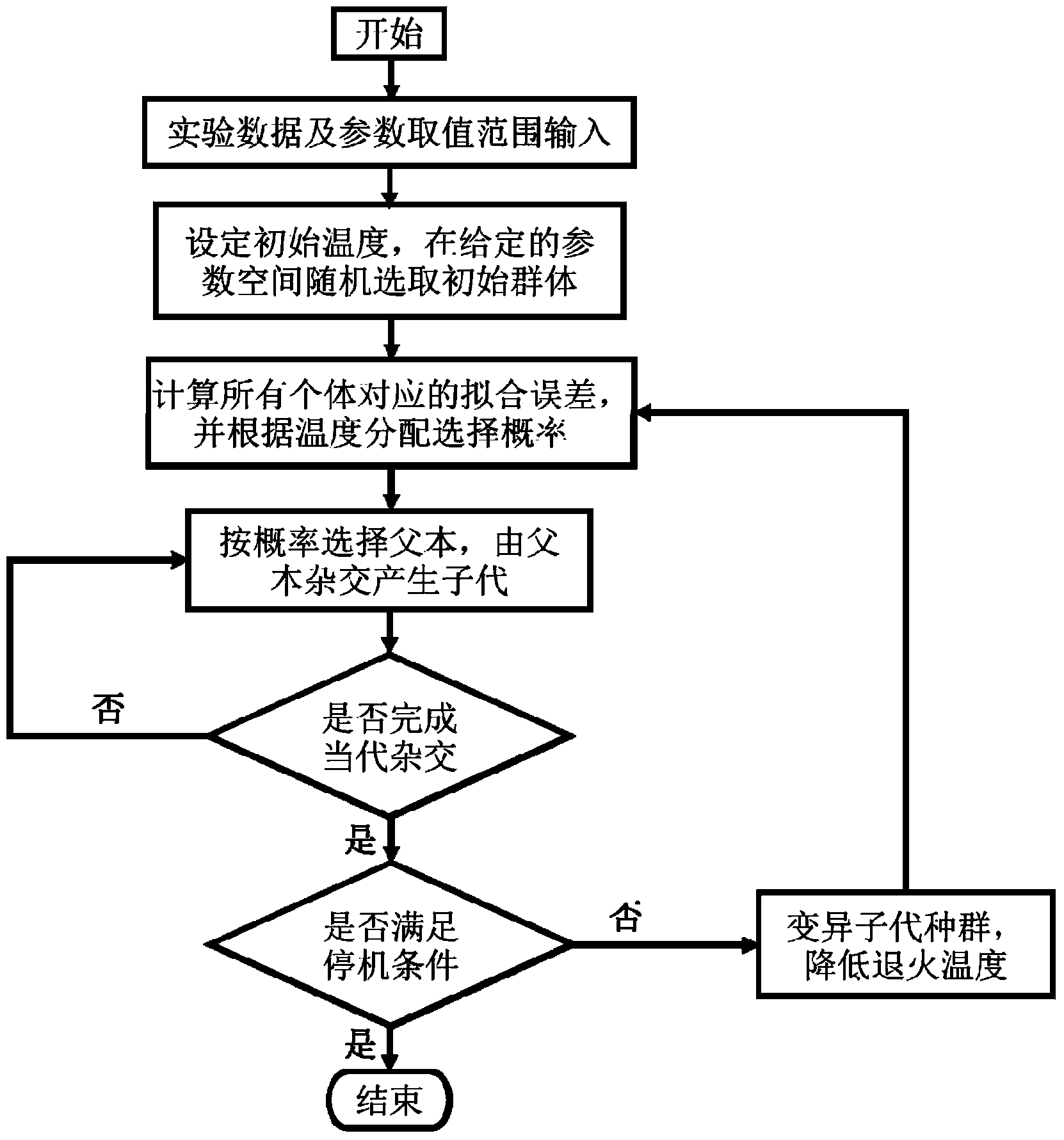
The invention discloses a metal-semiconductor contact nonlinear transmission line model and parameter fitting method and relates to the semiconductor device structure performance detection and representation field. The metal-semiconductor contact nonlinear transmission line model and parameter fitting method comprises 1, establishing a nonlinear transmission line model; 2, measuring an I-V curve of parallel double rectangular electrodes on semiconductor thin film materials; 3, obtaining an R-V curve through a relational expression that R is equal to dV / dI; 4, calculating a theoretical R-V curve of a testing structure through the nonlinear transmission line model; 5, fitting metal-semiconductor contact physical parameters through a simulated annealing inheritance algorithm. The metal-semiconductor contact nonlinear transmission line model and parameter fitting method has the advantages of establishing the nonlinear transmission line model and a corresponding numerical algorithm, quantitatively extracting the metal-semiconductor contact relevant physical parameters and providing a new method for precise representation and analysis of nonlinear metal-conductor contact.

Description

technical field [0001] The invention relates to the field of detection and characterization of the structural performance of semiconductor devices, specifically, it is to detect the physical parameters of the nonlinear metal-semiconductor contact, by measuring the I-V curve between two rectangular metal electrodes on the semiconductor film material, and then using the nonlinear transmission line The model fits the physical parameters of the metal-semiconductor contact. Background technique [0002] Metal-semiconductor contacts have been extensively studied due to their importance in DC, microwave applications, and as components of other semiconductor devices. The contact resistance between metal and semiconductor will affect the noise frequency characteristics, output power, thermal stability and reliability of semiconductor devices. Therefore, accurately describing the contact resistance between metal and semiconductor has become an important aspect to evaluate the perform...

Claims


Application Information

Patent Timeline
IPC IPC(8): G01R31/26
Inventor 何凯陈星李杨张勤耀王建新林春周松敏
Owner SHANGHAI INST OF TECHNICAL PHYSICS - CHINESE ACAD OF SCI
Learn More