

Optical communication device
An optical communication and mounting surface technology, applied in the field of optical communication, can solve the problems of large size of the optical coupling shell, unfavorable miniaturization, increase the size of the optical communication device, etc., and achieve the effect of reducing the size and being conducive to miniaturization
- Summary
- Abstract
- Description
- Claims
- Application Information
AI Technical Summary
Problems solved by technology
Method used
Image

Examples
Embodiment Construction
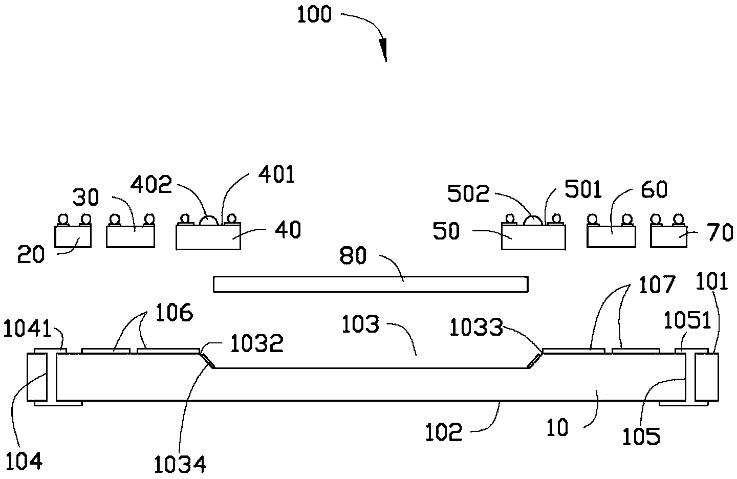
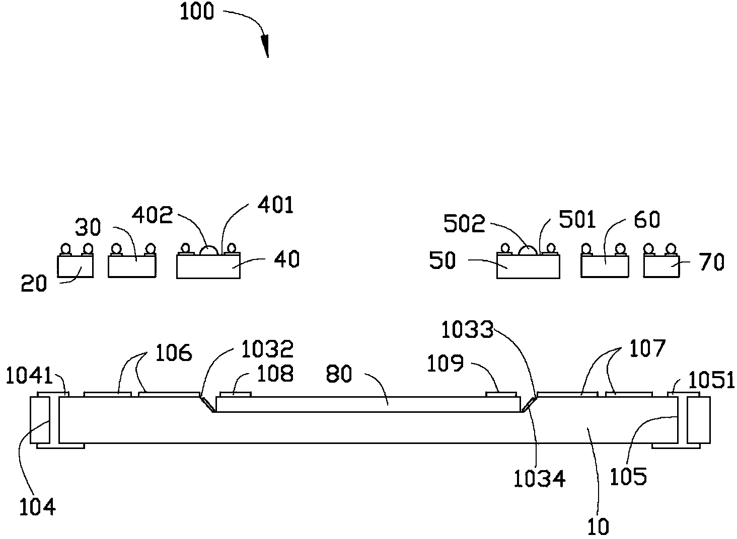
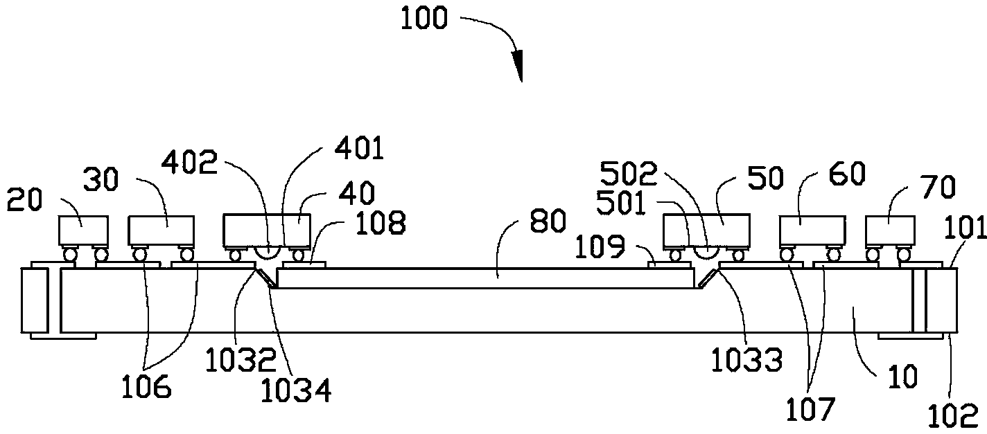
[0012] Such as figure 1 As shown, an optical communication device 100 provided for an embodiment of the present invention includes a circuit board 10, a processor 20, a first controller 30, a light emitting element 40, a light receiving element 50, a second control device 60, a memory 70 and a planar optical waveguide 80.
[0013] The circuit board 10 includes a mounting surface 101 and a lower surface 102 opposite to the mounting surface 101 . The installation surface 101 defines a groove 103 and a plurality of first through holes 104 and second through holes 105 penetrating through the installation surface 101 and the lower surface 102 . The groove 103 includes a bottom surface 1031 parallel to the installation surface 101 , a first slope 1032 inclined relative to the bottom surface 1031 , and a second slope 1033 inclined relative to the bottom surface 1031 . Both the first slope 1032 and the second slope 1033 are connected between the installation surface 101 and the bott...
PUM
 Abstract
Description
Claims
Application Information