Chip on film (COF) substrate and manufacturing method thereof and display panel

A technology of chip-on-chip film and manufacturing method, which is applied in the direction of metal pattern materials, optics, instruments, etc., can solve problems such as corrosion and affecting signal transmission, and achieve the effects of increasing service time, prolonging life, and reducing the risk of corrosion cracking

Inactive Publication Date: 2014-09-17
TCL CHINA STAR OPTOELECTRONICS TECH CO LTD
View PDF6 Cites 8 Cited by
  • Summary
  • Abstract
  • Description
  • Claims
  • Application Information

AI Technical Summary

Problems solved by technology

[0007] The object of the present invention is to provide a chip-on-chip film substrate and its manufacturing method and display panel, aiming to solve the existing problem in the prior art that the welding leads on the COF will be partially exposed in the air, but will be exposed in the environment where ions exist. Electrochemical reactions occur and will be corroded, thus affecting the transmission of signals

Method used


Image

  • Chip on film (COF) substrate and manufacturing method thereof and display panel
  • Chip on film (COF) substrate and manufacturing method thereof and display panel
  • Chip on film (COF) substrate and manufacturing method thereof and display panel

Examples


Embodiment Construction

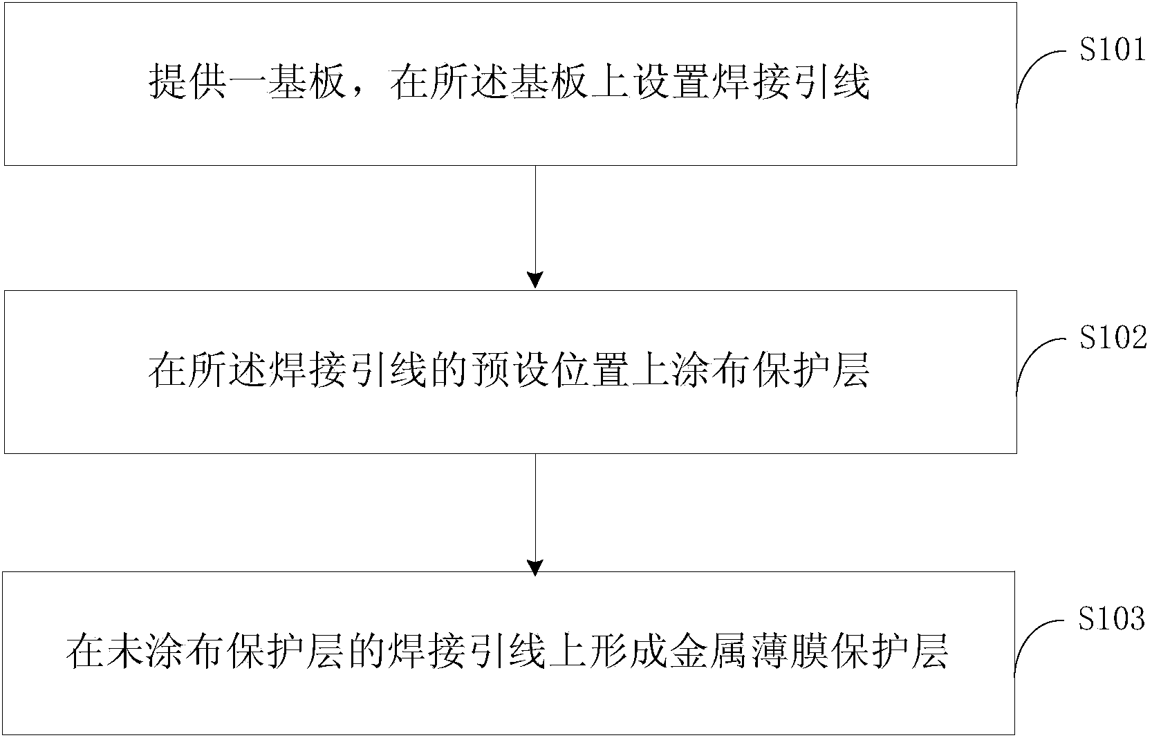
[0042] In order to make the object, technical solution and beneficial effects of the present invention more clear, the present invention will be further described in detail below in conjunction with the accompanying drawings and embodiments. It should be understood that the specific embodiments described here are only used to explain the present invention, not to limit the present invention.

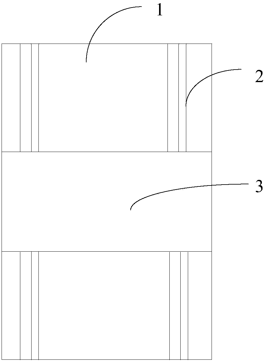
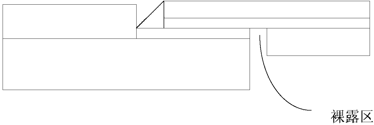
[0043] In the embodiment of the present invention, a layer of active metal thin film protective layer is plated on the welding leads exposed in the air on the COF substrate, which does not affect the conduction, but also protects the welding leads of copper material, and reduces the COF substrate. There is a risk of corrosion and fracture of the solder leads on the It solves the problem in the prior art that part of the welding lead on the COF is exposed in the air, but electrochemical reaction occurs in an environment where ions exist, and it will be corroded, thereby affecting the tran...


PUM


Abstract

The invention is suitable for the technical field of displays, and provides a chip on film (COF) substrate, which comprises a substrate, a protective layer and a metal film protective layer, wherein a welding wire is arranged on the surface of the substrate; the protective layer is arranged in the preset position of the welding wire; the metal film protective layer is arranged on the part, uncoated with the protective layer, of the welding wire. The active metal film protective layer is plated on the welding wire partially exposed in the air on the COF substrate, conduction is not affected, the time of copper corrosion is delayed, and the speed of copper corrosion is slowed. By applying the COF substrate and the manufacturing method thereof and the display panel, disclosed by the invention, the fracture risk of the welding wire on the COF substrate due to corrosion is effectively reduced, thus the using time of a product is increased, and the service life of the product is prolonged.

Description

technical field [0001] The invention belongs to the technical field of displays, and in particular relates to a chip-on-chip film substrate, a manufacturing method thereof, and a display panel. Background technique [0002] When the TFT-LCD (Thin Film Transistor Liquid Crystal Display, Thin Film Transistor Liquid Crystal Display) panel is displayed normally, it is necessary to use a COF substrate (chip on film, chip on film) to connect the PCB board (Printed Circuit Board, printed circuit board) and the LCD panel , so that the signals on the PCB can be conducted to the panel. [0003] Such as figure 1 As shown, a welding lead 2 is provided on a COF substrate 1 , and a protective layer 3 is coated on the welding lead 2 . Because copper has good electrical and thermal conductivity and good flexibility, copper is often used as a material for making welding leads. On the COF substrate, the welding leads not coated with the protective layer 3 are reserved for welding to the we...

Claims


Application Information

Patent Timeline
Patent Type & Authority Applications(China)
IPC IPC(8): G02F1/13G02F1/1333
CPCH05K1/09H05K1/118H05K1/189H05K3/34G02F1/1368G02F1/136222
Inventor 黄世帅
Owner TCL CHINA STAR OPTOELECTRONICS TECH CO LTD
Why Eureka
Try Eureka