Solar cell epitaxial wafer and its manufacturing method

A technology of solar cells and manufacturing methods, applied in the field of solar cells, can solve the problems of reducing the stripping speed and hindering the replenishment of acid solution, and achieve the effects of shortening the time, accelerating the corrosion speed, and reducing the corrosion time

Active Publication Date: 2017-09-29
SUZHOU JUZHEN PHOTOELECTRIC
View PDF5 Cites 0 Cited by
  • Summary
  • Abstract
  • Description
  • Claims
  • Application Information

AI Technical Summary

Problems solved by technology

In actual stripping, the gas generated by the corrosion reaction is easy to accumulate between the substrate and the GaAs cell layer, which hinders the acidic solution from replenishing to the reaction front and further reduces the stripping speed.

Method used


Image

  • Solar cell epitaxial wafer and its manufacturing method
  • Solar cell epitaxial wafer and its manufacturing method
  • Solar cell epitaxial wafer and its manufacturing method

Examples


Embodiment 1

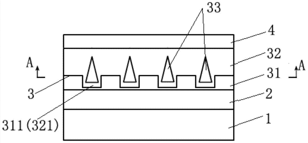
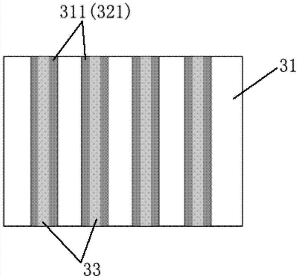
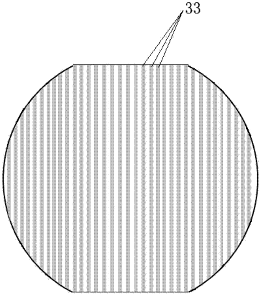
[0035] like figure 1 As shown, this embodiment provides a solar cell epitaxial wafer, including a substrate 1, a buffer layer 2, a sacrificial layer 3 and a solar cell layer 4 arranged in sequence, wherein the sacrificial layer 3 includes a first sacrificial layer 31 and a second sacrificial layer 31. Sacrificial layer 32, the first sacrificial layer 31 is arranged close to the buffer layer 2, the second sacrificial layer 32 is arranged close to the first sacrificial layer 31, a plurality of grooves 311 are distributed on the first sacrificial layer 31, and on the second sacrificial layer 32 There are a plurality of protrusions 321 that cooperate with the grooves 311, such as figure 2 As shown, the protrusion 321 has a gap 33 extending along the length direction of the groove 311 for allowing the etching solution to flow into the sacrificial layer 3 .

[0036] Specifically, the above-mentioned groove 311 may pass through the entire sacrificial layer 3 , or both ends of the g...

Embodiment 2

[0046] like Image 6 As shown, this embodiment provides a method for manufacturing a solar cell epitaxial wafer, for manufacturing the solar cell epitaxial wafer in the above-mentioned embodiment 1, comprising the following steps:

[0047] S1: growing the buffer layer 2 epitaxially on the substrate 1, specifically, metal organic compound chemical vapor phase epitaxy (MOCVD) can be used. The metal-organic compound chemical vapor phase epitaxy technology is currently the most mature epitaxial growth technology with the best effect in the manufacture of III-V compound solar cells. In addition, molecular beam epitaxy (MBE) with a slower growth rate can also be selected.

[0048] S2: Epitaxially grow the first sacrificial layer 31 on the buffer layer 2, such as Figure 7 As shown, specifically, metal organic compound chemical vapor phase epitaxy (MOCVD) can be used.

[0049] S3: Etch a plurality of grooves 311 on the first sacrificial layer 31, such as Figure 8 As shown, the gr...


PUM


Abstract

The invention provides a solar cell epitaxial wafer and a manufacturing method thereof. The solar cell epitaxial wafer comprises a substrate, a buffer layer, sacrificial layers and a solar cell layer, wherein the substrate, the buffer layer, the sacrificial layers and the solar cell layer are sequentially disposed. The sacrificial layers comprise a first sacrificial layer and a second sacrificial layer. The first sacrificial layer is arranged to cling to the buffer layer. The second sacrificial layer is arranged to cling to the first sacrificial layer. The first sacrificial layer is provided with a plurality of grooves. The second sacrificial layer is provided with a plurality of projections matched with the grooves. The projections are internally provided with gaps that extend along the length direction of the grooves. By means of the plurality of gaps in the sacrificial layers, when the solar cell epitaxial wafer is immersed in a selective etching solution, the selective etching solution can enter the interior of the solar cell epitaxial wafer through the edges of the sacrificial layers via the above gaps. In this way, the etching speeds of the sacrificial layers are accelerated. Therefore, the duration of the epitaxy lift-off step during the manufacturing process of solar cells is reduced.

Description

technical field [0001] The invention relates to the technical field of solar cells. Specifically, it relates to a solar cell epitaxial wafer and a manufacturing method thereof. Background technique [0002] GaAs solar cell technology is developing rapidly, and its application fields have gradually expanded from space applications to ground applications. It has broad market prospects in the fields of portable energy and consumer electronics. Using epitaxial lift-off technology (ELO technology) to make GaAs solar cells, on the one hand, the GaAs substrate can be reused after peeling off, which can significantly reduce product costs; on the other hand, flexible GaAs solar cells can be made, and the efficiency is not only improved compared to before stripping , and the product is lighter and flexible, which is more conducive to aerospace and portable applications, etc., and has a wide range of uses. [0003] In the prior art, the process of making GaAs solar cells using epitax...

Claims


Application Information

Patent Timeline
Patent Type & Authority Patents(China)
IPC IPC(8): H01L31/0352H01L31/18
CPCH01L31/035281H01L31/1892Y02E10/50Y02P70/50
Inventor 黄添懋杨晓杰刘凤全叶继春
Owner SUZHOU JUZHEN PHOTOELECTRIC
Why Eureka
Try Eureka