Method and device for operation of FPGA (Field Programmable Gate Array) in MCU (Microprogrammed Control Unit) chip

A technology of chips and flash memory chips, which is applied in the field of devices where FPGA works in MCU chips, can solve the problems of large FPGA area, difficulty in meeting demands, and increased costs, and achieve the effects of reducing area, reducing waste, and improving stability

Active Publication Date: 2014-09-17
GIGADEVICE SEMICON (BEIJING) INC
View PDF8 Cites 12 Cited by
  • Summary
  • Abstract
  • Description
  • Claims
  • Application Information

AI Technical Summary

Problems solved by technology

[0005] However, the complete FPGA has a large area. When integrated into the MCU chip, it needs to increase the chip's very large area, resulting in an increase in cost. Moreover, the complete FPGA contains some unnecessary components, resulting in waste. More importantly, When it is necessary to realize that the circuits in the FPGA and other parts of the MCU chip work together, because the work of the FPGA and the MCU chip is not related to each other, this requirement is difficult to achieve

Method used


Image

  • Method and device for operation of FPGA (Field Programmable Gate Array) in MCU (Microprogrammed Control Unit) chip
  • Method and device for operation of FPGA (Field Programmable Gate Array) in MCU (Microprogrammed Control Unit) chip
  • Method and device for operation of FPGA (Field Programmable Gate Array) in MCU (Microprogrammed Control Unit) chip

Examples


Embodiment Construction

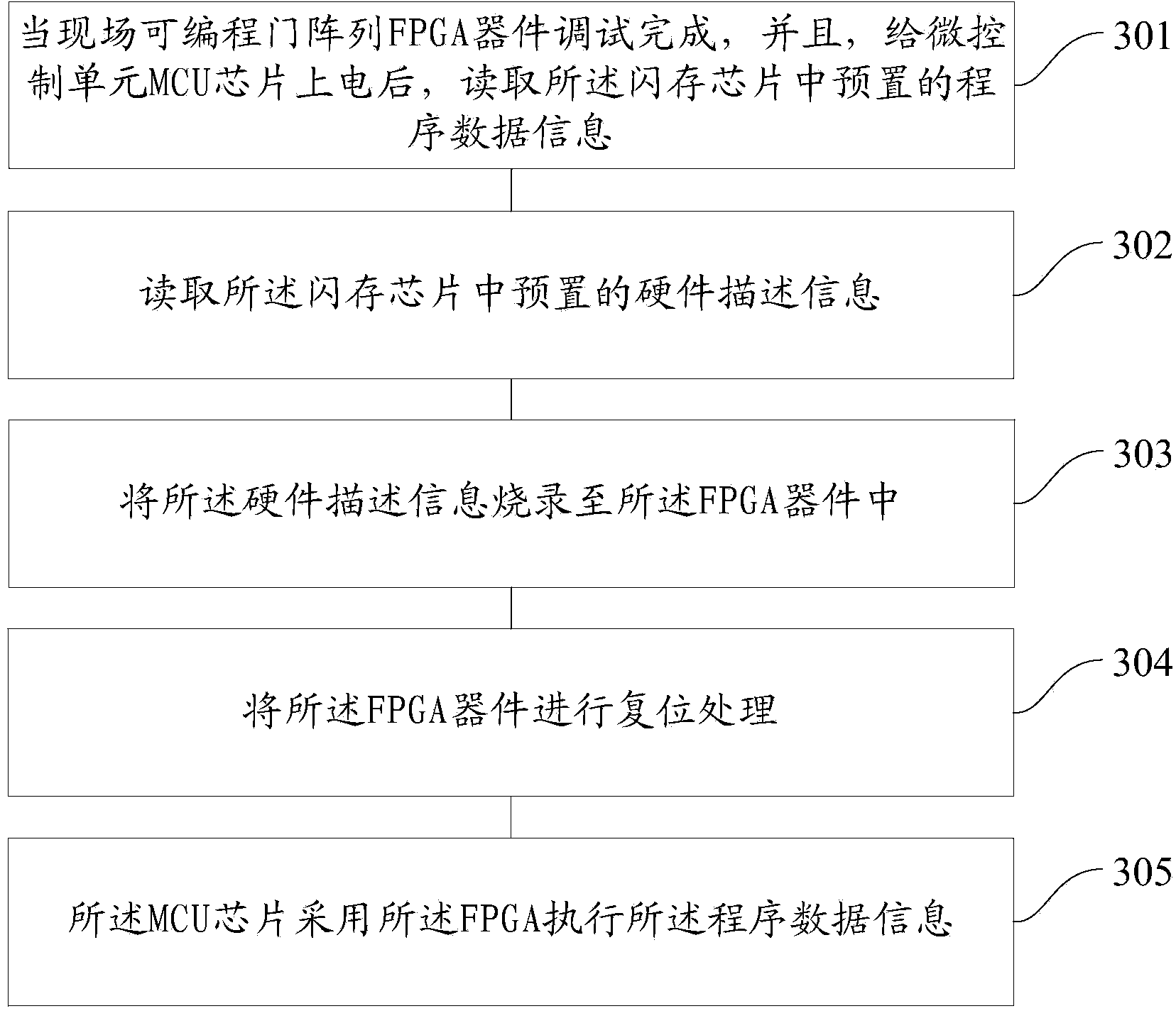
[0060] In order to make the above objects, features and advantages of the present invention more comprehensible, the present invention will be further described in detail below in conjunction with the accompanying drawings and specific embodiments.

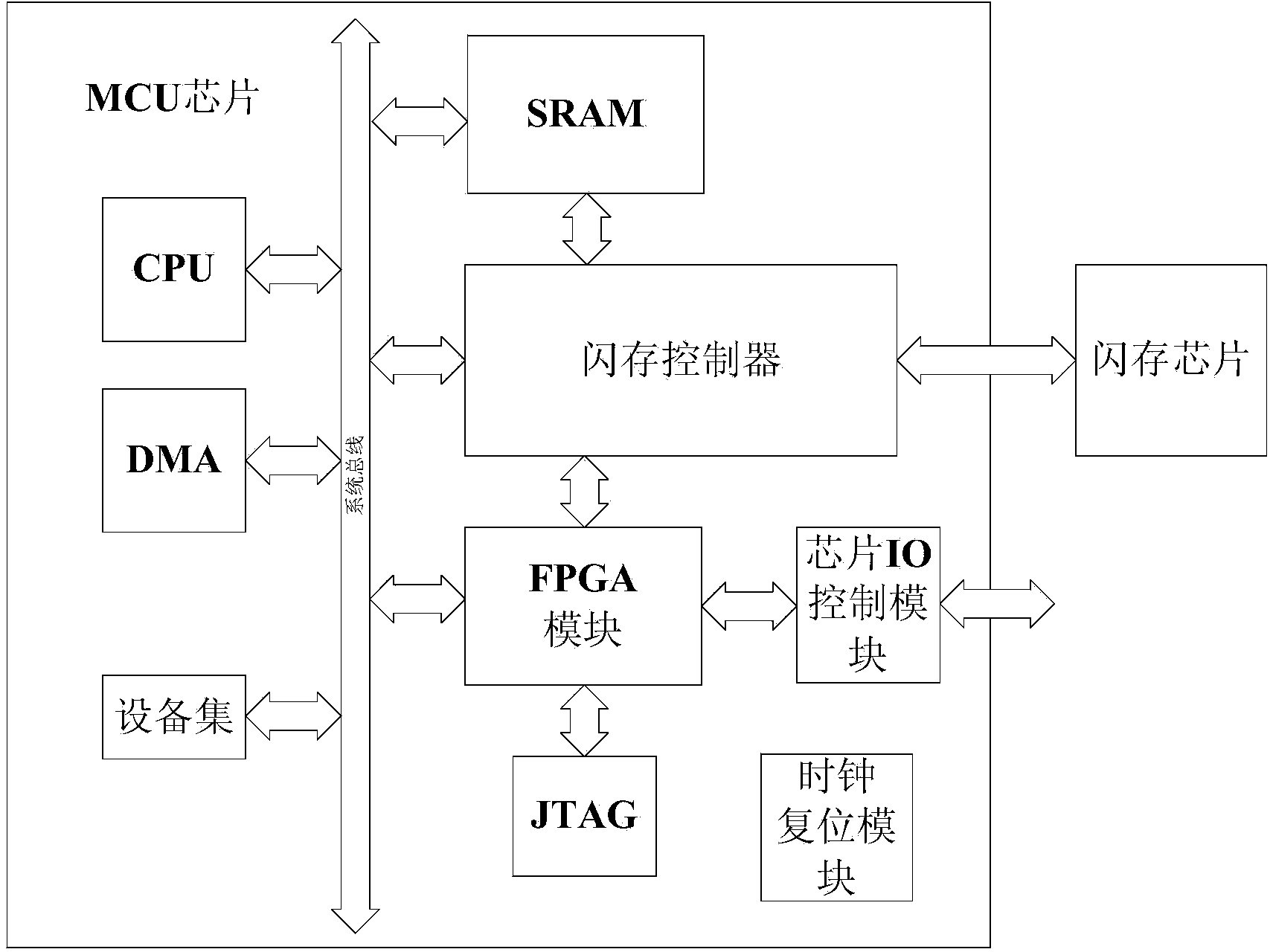
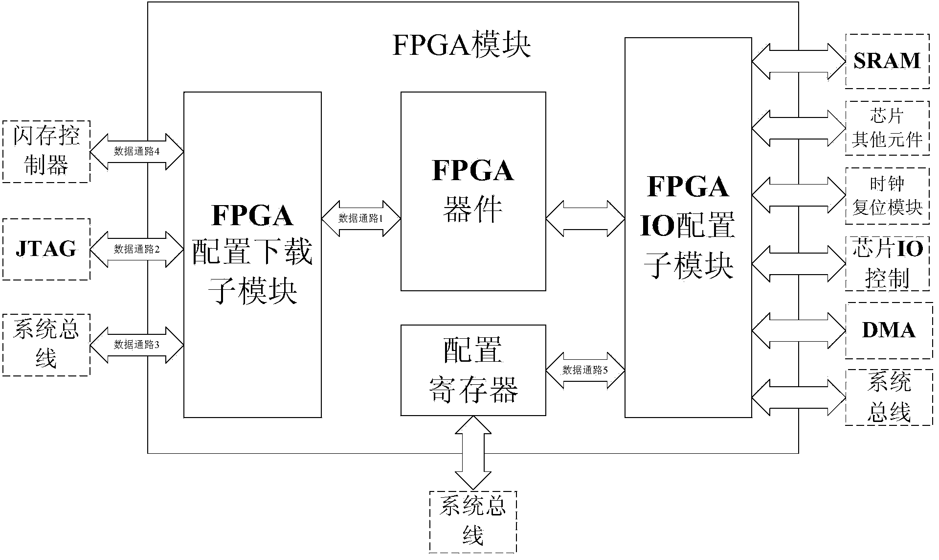
[0061] refer to figure 1 , shows a structural diagram of a micro control unit MCU chip integrating a field programmable gate array FPGA module of the present invention.

[0062] Such as figure 1 As shown, the MCU chip is integrated with a field programmable gate array FPGA module, and the MCU chip also includes:

[0063] CPU, system bus, chip IO control module and clock reset module, wherein,

[0064] The CPU and the FPGA module are respectively connected to the system bus; the clock reset is interconnected with the FPGA module;

[0065] In practical applications, the CPU (Central Processing Unit, central processing unit) is generally an IP core (Intellectual Property Core, intellectual property core). The so-called IP core is ...


PUM


Abstract

The embodiment of the invention provides a method and a device for the operation of an FPGA (Field Programmable Gate Array) in an MCU (Microprogrammed Control Unit) chip. An FPGA module and a flash chip are integrated in the MCU chip, the FPGA module comprises an FPGA component and an FPGA IO (Input/Output) configuration submodule, and the FPGA IO configuration submodule is respectively connected with all elements in the MCU chip. The method includes the following steps: after the FPGA component is debugged and the MCU chip is electrified, the program data information preset in the flash chip is read; the hardware description information preset in the flash chip is read; the hardware description information is burnt into the FPGA component; the FPGA component is reset; the MCU chip adopts the FPGA to execute the program data information. The cost and waste can be reduced, and the condition that the circuit in the FPGA and the other circuits of the MCU chip can cooperatively work can also be ensured.

Description

technical field [0001] The invention relates to the technical field of integrated circuits, in particular to a method for FPGA working in an MCU chip and a device for FPGA working in an MCU chip. Background technique [0002] With the continuous improvement of integrated circuit technology, field programmable gate array FPGA (Field-Programmable Gate Array) appears as a semi-custom circuit in the field of application-specific integrated circuit (ASIC, Application-Specific Integrated Circuit), the logic block of FPGA And the connection can be changed according to the user's needs, and the logic blocks inside the FPGA can be connected through editable connections, so the FPGA can complete the required logic functions. [0003] Due to the extremely high flexibility of FPGA, MCU (Micro Control Unit, Micro Control Unit) chip manufacturers hope to integrate FPGA into MCU chips to solve the contradiction of different functional requirements of MCU chips in different application scen...

Claims


Application Information

Patent Timeline
Patent Type & Authority Applications(China)
IPC IPC(8): G06F11/26
Inventor 王南飞李宝魁
Owner GIGADEVICE SEMICON (BEIJING) INC
Why Eureka
Try Eureka