

Communication device and method for realizing communication between DSP and PC by means of PCIE on basis of FPGA
A communication device and bus signal technology, applied in the field of communication, can solve problems such as lack of flexibility, and achieve the effects of increased flexibility, simple structure, and flexible communication
- Summary
- Abstract
- Description
- Claims
- Application Information
AI Technical Summary
Problems solved by technology
Method used
Image

Examples
specific Embodiment approach 1
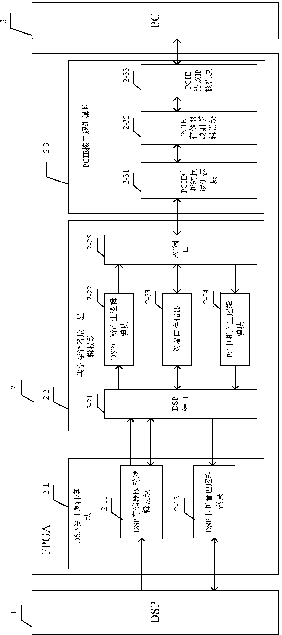
[0043] Specific implementation mode one: refer to figure 1 Specifically illustrate this embodiment, a kind of communication device that realizes DSP and PC to communicate by PCIE bus based on FPGA described in this embodiment, it comprises: FPGA2;
[0044] The DSP logic signal output end of DSP1 is connected to the DSP logic signal input end of FPGA2, the DSP logic signal input and output end of DSP1 is connected to the DSP logic signal input and output end of FPGA2, and the PCIE bus signal input and output end of FPGA2 is connected to the signal input and output end of PC3;
[0045] Described FPGA2 comprises: DSP interface logic module 2-1, shared memory interface logic module 2-2 and PCIE interface logic module 2-3;
[0046]The DSP logic signal input terminal of the DSP interface logic module 2-1 is used as the DSP logic signal input terminal of FPGA2, the DSP logic signal input and output terminals of the DSP interface logic module 2-1 are used as the DSP logic signal input...
specific Embodiment approach 2
[0070] Specific embodiment two: this embodiment is a kind of communication device that realizes DSP and PC to communicate by means of PCIE bus based on FPGA described in specific embodiment one and is described further, and in this embodiment, described shared memory interface logic module 2 -2 also includes: DSP port module 2-21 and PC port module 2-25;
[0071] The interrupt signal input end of the DSP port module 2-21 is used as an interrupt signal input end of the shared memory interface logic module 2-2, and a storage signal input and output end of the DSP port module 2-21 is used as a shared memory interface logic module 2-2. A storage signal input and output terminal, the interrupt trigger signal output terminal of the DSP port module 2-21 is used as an interrupt trigger signal output terminal of the shared memory interface logic module 2-2;
[0072] The interrupt signal output end of the PC port module 2-25 is used as another interrupt trigger signal output end of the ...
specific Embodiment approach 3
[0075]Specific embodiment three: this embodiment is to further illustrate a kind of communication device that realizes DSP and PC to communicate by PCIE bus based on FPGA described in specific embodiment two, in this embodiment, the signal input and output terminal of DSP1 and FPGA2 The external memory signal input and output terminals are connected through the EMIF interface.
[0076] The EMIF interface is an external memory connection interface.
PUM
 Abstract
Description
Claims
Application Information