Method for preventing soldering holes from being blocked in wave soldering process and printed circuit board

A technology for printed circuit boards and soldering holes, which is applied to printed circuit parts, assembled printed circuits with electrical components, and electrically connected printed components. It can solve problems such as labor and efficiency loss, tin accumulation, and hole blocking.

Inactive Publication Date: 2014-10-01
SHENZHEN GONGJIN ELECTRONICS CO LTD
View PDF5 Cites 5 Cited by
  • Summary
  • Abstract
  • Description
  • Claims
  • Application Information

AI Technical Summary

Problems solved by technology

The main reason is that there is no detinning pad, which will cause too much tin to accumulate on the pad, resulting in hole blocking
If ...

Method used


Image

  • Method for preventing soldering holes from being blocked in wave soldering process and printed circuit board
  • Method for preventing soldering holes from being blocked in wave soldering process and printed circuit board

Examples


Embodiment Construction

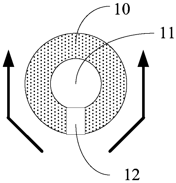
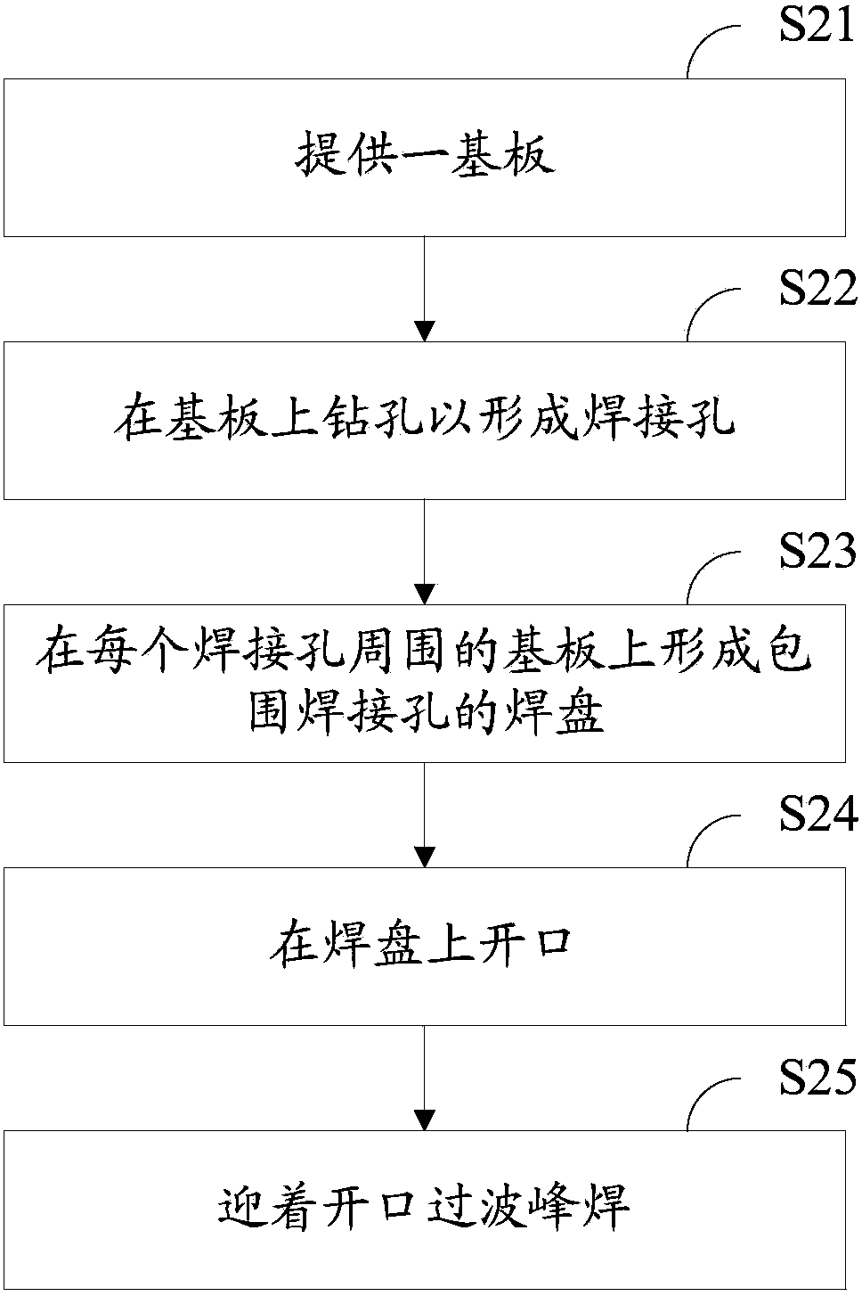
[0017] In order to facilitate the understanding of the present invention, the present invention will be described more fully below with reference to the associated drawings. A preferred embodiment of the invention is shown in the drawings. However, the present invention can be embodied in many different forms and is not limited to the embodiments described herein. Rather, these embodiments are provided so that the disclosure of the present invention will be thorough and complete.

[0018] It should be noted that when an element is referred to as being “fixed” to another element, it can be directly on the other element or there can also be an intervening element. When an element is referred to as being "connected to" another element, it can be directly connected to the other element or intervening elements may also be present. The terms "vertical," "horizontal," "left," "right," and similar expressions are used herein for purposes of illustration only.

[0019] Unless otherw...


PUM

PropertyMeasurementUnit
Widthaaaaaaaaaa

Abstract

The invention discloses a method for preventing soldering holes from being blocked in the wave soldering process. The method includes the following steps that a substrate is provided; holes are drilled in the substrate so as to form the soldering holes; a bonding pad enclosing each soldering hole is formed in the portion, around the soldering hole, of the substrate; an opening is formed in at least one bonding pad and covered with green oil; wave soldering is conducted towards the opening. The invention further relates to a printed circuit board. Because the opening of the bonding pad is covered with the green oil so that soldering tin cannot flow through in the wave soldering process, the soldering tin can only flow along the two sides of the opening and is not prone to flowing into the soldering holes, and thus it is guaranteed that the soldering holes without inserts cannot be blocked by the soldering tin easily in the wave soldering process.

Description

technical field [0001] The invention relates to the field of printed circuits, in particular to a method for preventing plugging of welding holes during wave soldering, and also to a printed circuit board. Background technique [0002] On the printed circuit board (PCB), there are often some plug-ins that are not loaded during wave soldering, and the corresponding pads are usually of a normal design. After the wave soldering, the soldering holes may be covered by tin. The main reason is that there is no detinning pad, which will cause too much tin to accumulate on the pad, resulting in hole blocking. If the hole needs to be installed later, it needs to be manually detinned to open the hole, resulting in a loss of labor and efficiency. Contents of the invention [0003] Based on this, it is necessary to provide a method for preventing soldering holes from being blocked during wave soldering. [0004] A method for preventing plugging of soldering holes during wave solderin...

Claims


Application Information

Patent Timeline
IPC IPC(8): H05K3/34H05K1/11
Inventor 王达国
Owner SHENZHEN GONGJIN ELECTRONICS CO LTD
Why Eureka
Try Eureka