Far-field light-field full-vector calculating method

A technology of full vector calculation and calculation method, which is applied in the field of calculation of far-field light field, and can solve problems such as inability to give far-field light field, occupying a large operating memory, and inability to give far-field results, etc.

Active Publication Date: 2014-10-08
BEIJING INSTITUTE OF TECHNOLOGYGY
View PDF6 Cites 2 Cited by
  • Summary
  • Abstract
  • Description
  • Claims
  • Application Information

AI Technical Summary

Problems solved by technology

However, because only one component of the light field is considered, the obtained results are only approximate results, which can be used in the design of traditional large optical devices, but cannot give accurate far-field results in the design of micro-nano optical devices.
However, the full

Method used


Image

  • Far-field light-field full-vector calculating method
  • Far-field light-field full-vector calculating method
  • Far-field light-field full-vector calculating method

Examples


Embodiment Construction

[0018] Embodiments of the present invention will be further described in detail below in conjunction with the accompanying drawings and examples. The following examples are used to illustrate the present invention, but should not be used to limit the scope of the present invention.

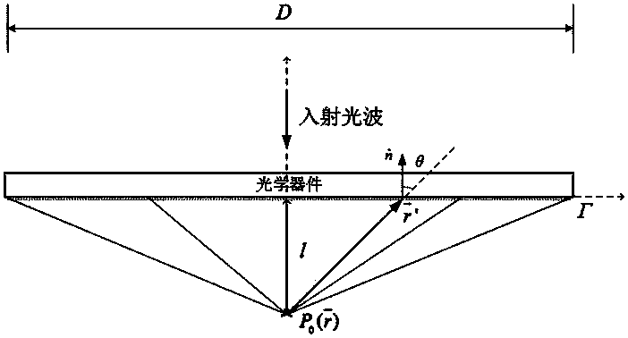
[0019] This embodiment provides a schematic diagram of a far-field light field full vector calculation method, as shown in figure 1 As shown, P 0 The point is a certain point in the far field, which is the required position of the light field. The width of the optic is D. This calculation method can be divided into two steps:

[0020] In the first step, the light field distribution of the light field passing through a certain near-field plane Γ of the optical device is obtained through the traditional full vector calculation method. The near-field light field distribution of the optical device can be obtained by using any full vector calculation method such as finite time domain difference or ...


PUM


Abstract

The invention relates to a far-field light-field full-vector calculating method. After near-field distribution of an optical device is obtained through other full-vector calculation methods, distribution of any point of an optical-field far field is obtained through a full-vector integral method so that precision of full-vector calculation is reserved and speed and far-field calculability of a diffraction algorithm are also realized. The calculation result is more accurate than a scalar approximation method and not only intensity of the far-field light field can be calculated accurately, the phase of the far-field light field can also be calculated accurately. At the same time, because an integral formula is significantly small in occupied memory and unrelated with a far-field distance, a far field which cannot be calculated through other full-vector methods can be calculated so that the method has the advantages of being rapid and efficient. The method is widely applicable to the field of optics.

Description

technical field [0001] The invention relates to a calculation method of a light field, in particular to a calculation method of a far-field light field. Background technique [0002] With the continuous improvement of micro-nano processing technology, optical devices are becoming more and more miniaturized and integrated. The size of existing optical devices can reach the order of microns or even nanometers, and nanoscale optical manipulation that breaks through the diffraction limit can be realized, thereby realizing functions that cannot be accomplished by traditional optical devices. In the design process of this type of micro-nano optical device, it is necessary to calculate the light field modulated by the optical device first, check whether the light field meets people's design goals, and then continuously adjust the parameters of the optical device until the light field reaches the target. device design. Therefore, an accurate and fast light field calculation method...

Claims


Application Information

Patent Timeline
IPC IPC(8): G02B27/00
Inventor 胡滨刘娟王涌天韩剑
Owner BEIJING INSTITUTE OF TECHNOLOGYGY
Why Eureka
Try Eureka