
A Current Mirror for Low Supply Voltage

A technology of low power supply voltage and current mirror, applied in the field of current mirror, can solve the problems of reduced voltage margin and inappropriate current mirror circuit

Inactive Publication Date: 2015-11-25
UNIV OF ELECTRONICS SCI & TECH OF CHINA
View PDF6 Cites 0 Cited by
  • Summary
  • Abstract
  • Description
  • Claims
  • Application Information

AI Technical Summary

Problems solved by technology

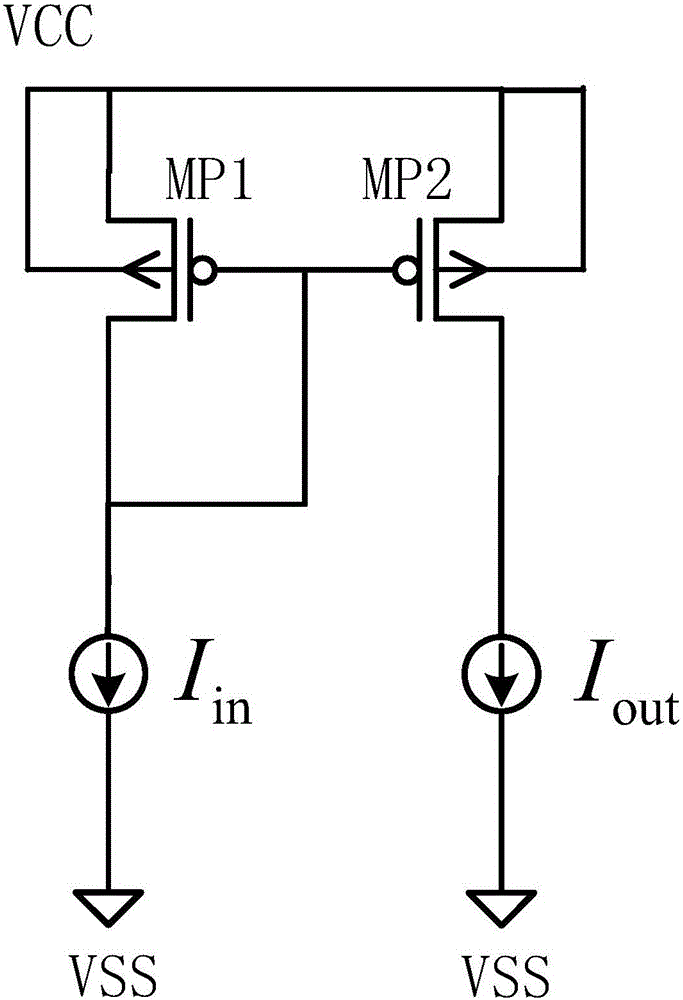
It can be seen from the above two equations that V SD1 than the overdrive voltage V of the MP1 tube OV1 The absolute value of the threshold voltage of a PMOS transistor MP1 is larger, which leads to a reduction in voltage margin, so this traditional current mirror circuit is not suitable for working at low power supply voltages

Method used


Image

  • A Current Mirror for Low Supply Voltage
  • A Current Mirror for Low Supply Voltage
  • A Current Mirror for Low Supply Voltage

Examples


Embodiment Construction

[0013] The specific embodiment of the present invention is described below in conjunction with accompanying drawing

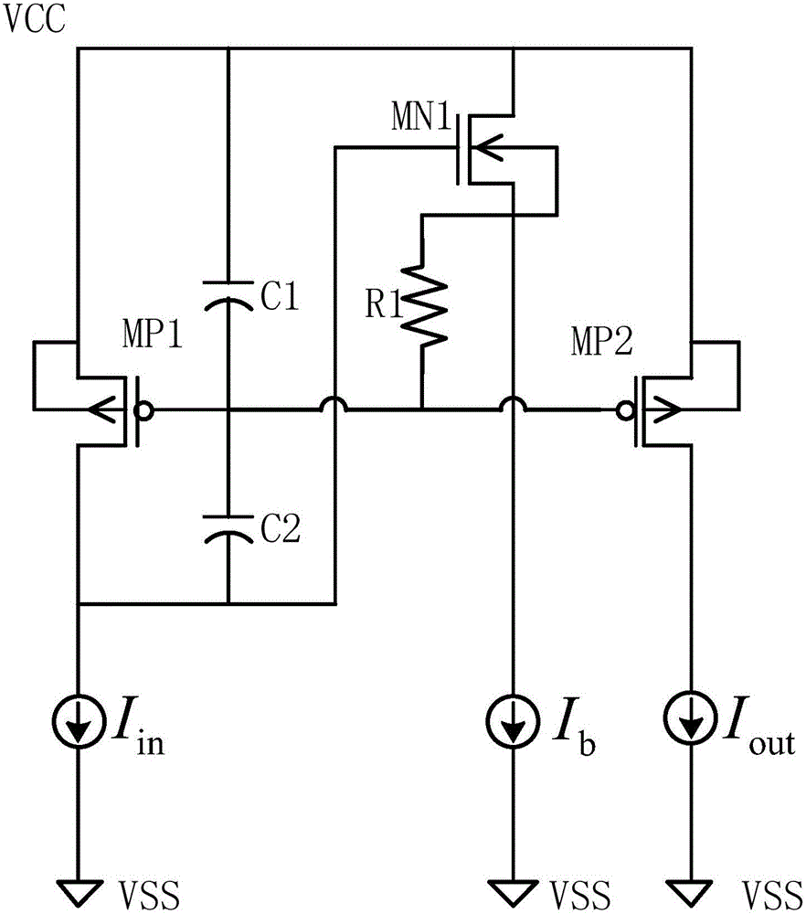
[0014] Such as figure 2 As shown, the current mirror of the present invention is composed of PMOS transistors MP1, MP2, NMOS transistor MN1, capacitors C1, C2, resistor R1, input current source, output terminal current source and bias current source; wherein, the source of MP1 is connected to Power supply VCC, its gate is connected to the gate of MP2, its drain is connected to the positive pole of the input current source; the negative pole of the input current source is grounded to VSS; the drain of MN1 is connected to the power supply VCC, its gate is connected to the positive pole of the input current source, and its source The pole is connected to the positive pole of the bias current source, and its substrate is connected to the connection point between the gate of MP1 and the gate of MP2 through R1; the negative pole of the bias current source is grounde...


PUM


Abstract

The invention relates to the technical field of integrated circuits, in particular to a current mirror. The current mirror is characterized in that the current mirror is composed of a PMOS transistor MP1, a PMOS transistor MP2, an NMOS transistor MN1, a capacitor C1, a capacitor C2, a resistor R1, an input current source, an output end current source and a bias current source. The source electrode of the MP1 is connected with a power source VCC, the grid electrode of the MP1 is connected with the grid electrode of the MP2, and the drain electrode of the MP1 is connected with positive electrode of the input current source. The negative electrode of the input electrode source is grounded VSS. The drain electrode of the MN1 is connected with the power source VCC, the grid electrode of the MN1 is connected with the positive electrode of the input current source, the source electrode of the MN1 is connected with the positive electrode of the bias current source, and the substrate of the MN1 is connected with a connection point of the grid electrode of the MP1 and the grid electrode of the MP2 through the R1. A connection point of the source electrode of the MP1 and the drain electrode of the MN1 is connected with a connection point of the grid electrode of MN1 and the positive electrode of the input current source through the C1 and the C2 sequentially. The source electrode of the MP2 is connected with the power source VCC, and the drain electrode of the MP2 is connected with the positive electrode of an output current source. The current mirror has the advantages of being suitable for being used under low supply voltage, meanwhile improving the PSR of the current mirror, and being especially suitable for a current mirror circuit.

Description

technical field [0001] The invention relates to the technical field of integrated circuits, in particular to a current mirror. Background technique [0002] A current mirror is an important circuit unit in an analog circuit. It can be used as a bias unit or a signal processing unit, and is widely used in analog circuits and radio frequency circuits. [0003] figure 1 is a schematic diagram of an existing current mirror circuit, the input current source I in , output current source I out Composed of PMOS transistors MP1 and MP2. Among them, the gate and drain of the MP1 tube are short-circuited, so the overdrive voltage of the MP1 tube is: [0004] V OV1 =V SG1 -|V THP1 | [0005] The source-drain voltage of the MP1 tube is: [0006] V SD1 =V SG1 [0007] where |V THP1 | is the absolute value of the threshold voltage of the PMOS transistor MP1, V SG1 It is the voltage between source and gate of MP1 tube. It can be seen from the above two equations that V SD1 t...

Claims


Application Information

Patent Timeline
Patent Type & Authority Patents(China)
IPC IPC(8): G05F3/26
Inventor 王卓赵倬毅石跃董渊柯普仁周泽坤张波
Owner UNIV OF ELECTRONICS SCI & TECH OF CHINA
Learn More