
Substrate and process for mounting chip on substrate

A substrate and chip technology, which is applied in the direction of electrical components, electric solid devices, circuits, etc., can solve the problems of high surface flatness requirements of substrate pads, failure of solder joints of LED chips in formal installation, and yellowing of substrate reflective layers, etc., to achieve improved Solder joint reliability, reduced risk of solder joint failure, effect of reduced porosity

Inactive Publication Date: 2014-10-08
北京国联万众半导体科技有限公司
View PDF4 Cites 7 Cited by
  • Summary
  • Abstract
  • Description
  • Claims
  • Application Information

AI Technical Summary

Problems solved by technology

However, since the AuSn plating layer on the electrode of the LED chip has a thickness of only about 5 μm, the requirements for the surface flatness of the substrate pad are relatively high.
Otherwise, it is easy to produce the problem of solder joint holes, especially for flexible substrates, which is very unfavorable
At the same time, the AuSn reflow soldering process requires a temperature of 300-320°C, which is too high for a flexible substrate, and may easily lead to problems such as pad warping and yellowing of the reflective layer of the substrate.
However, if BGA reflow soldering is also used, the above-mentioned problems of solder joint failure and chip inclination for the formal LED chip still exist.

Method used


Image

  • Substrate and process for mounting chip on substrate
  • Substrate and process for mounting chip on substrate
  • Substrate and process for mounting chip on substrate

Examples


Embodiment Construction

[0030] The present invention will be further described below with regard to the method for mounting LED chips on a flexible substrate and the flexible substrate formed therefrom. However, those skilled in the art can understand that the present invention is not limited to mounting LED chips on a flexible substrate, but can be extended to mounting any type of electronic chip on any substrate.

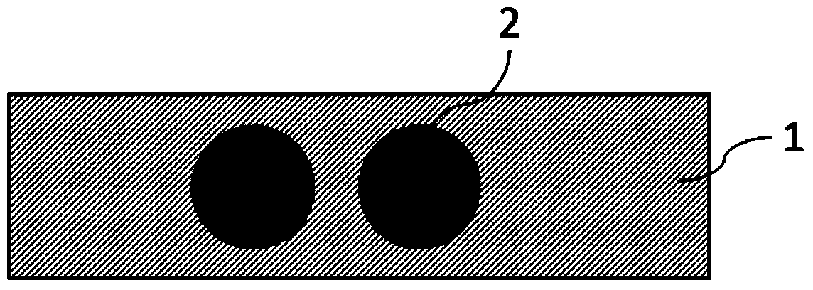
[0031] figure 1 Schematically shows an LED chip 5 to be mounted on a flexible substrate, which is, for example, a front-mounted LED chip. As shown in the figure, the LED chip 5 includes two spaced apart electrodes 6 . The electrodes are used to connect with the flexible substrate. In a non-limiting embodiment, the size of the electrodes 6 is about 100 μm, the distance between the two electrodes is greater than 150 μm, and there is a height difference between them of 5-15 μm. The material of the surface layer of the electrode 6 is usually Au.

[0032] Figure 2a A substrate 1 is show...


PUM


Abstract

The invention relates to a substrate and a process for mounting a chip on the substrate. The substrate comprises a substrate body and a chip mounted on the substrate body, wherein pads of a solder layer are arranged on the substrate body, and the chip has electrodes connected to the pads. The pads are configured to be larger than the electrodes. Therefore, after solder melts, even if drum-shaped solder joints appear, a firm bonding surface and firm bonding force can be provided, and the risk of solder joint failure is greatly reduced. In addition, because the area of the pads is increased, the area of the solder coating the pads is increased. Therefore, the design can increase the binding force between the solder and the pads and reduce the occurrence of reliability decline caused by interface deterioration. In addition, by appropriately choosing the sizes of the pads, possible chip tilt after an LED chip is mounted on a flexible substrate can be effectively avoided, the porosity is reduced, and the reliability of solder joints can be improved.

Description

technical field [0001] The invention relates to a substrate, in particular to a flexible substrate on which a chip, especially a light emitting diode (LED) is installed. The present invention also relates to a process for mounting chips on a substrate, especially a process for mounting LED chips on a flexible substrate. Background technique [0002] Chips need to be mounted on substrates in the production of various electronic devices. For example, with the increasing popularity of light emitting diodes (LEDs), it is often necessary to mount LED chips on flexible substrates. [0003] Traditionally, LED chips mounted on flexible substrates are roughly divided into two types, namely front-mounted LED chips and flip-chip LED chips. For front-mounted LED chips, it is hoped that the bonding process can be saved by using flip-chip welding, avoiding lead wire shading, and improving heat dissipation performance. However, since there is a certain height difference (for example, ab...

Claims


Application Information

Patent Timeline
Patent Type & Authority Applications(China)
IPC IPC(8): H01L23/12H01L21/58
CPCH01L2224/10
Inventor 刘洋韦嘉崔成强袁长安
Owner 北京国联万众半导体科技有限公司
Learn More